

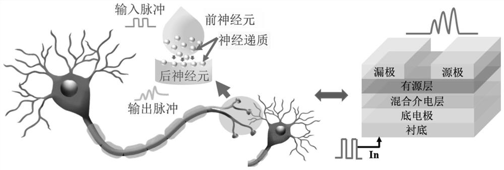
Low-voltage driving ink-jet printing flexible synaptic transistor and preparation method thereof
An inkjet printing, low-voltage drive technology, applied in the direction of transistors, semiconductor/solid-state device manufacturing, semiconductor devices, etc., to achieve excellent performance, low operating temperature, and convenient process preparation
- Summary
- Abstract
- Description
- Claims
- Application Information
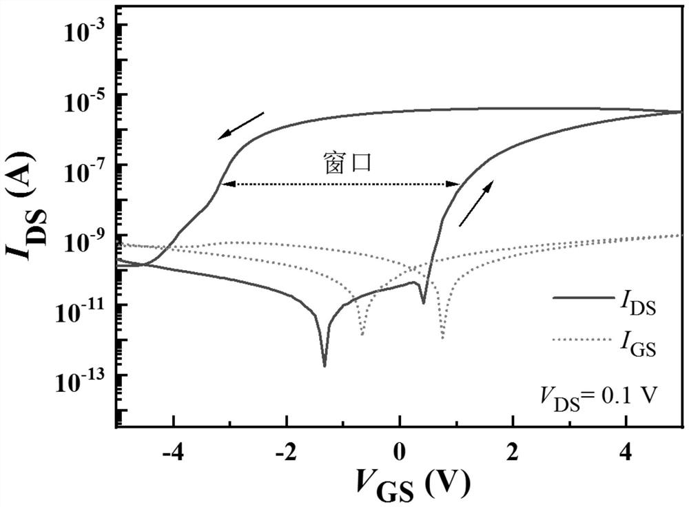
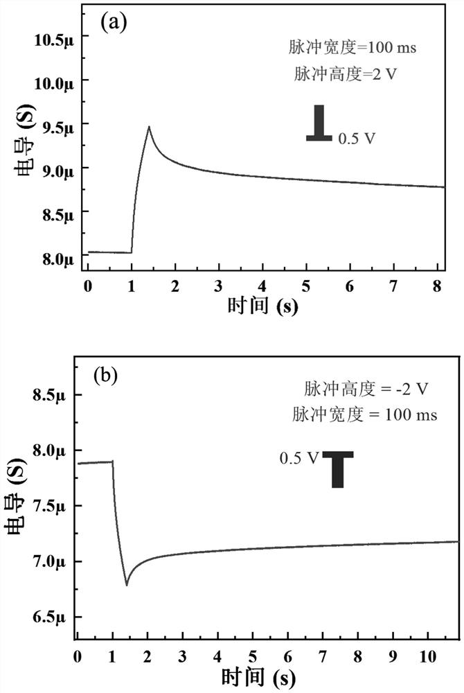
AI Technical Summary
Problems solved by technology
Method used
Image

Examples
preparation example Construction
[0030] The preparation method of the low voltage driven inkjet printing flexible synaptic transistor comprises the following steps:
[0031] S1. Prepare the substrate: form a buffer layer on the surface of the flexible substrate to make a substrate for use.
[0032] S2. Prepare the bottom electrode on the substrate: deposit the bottom electrode on the substrate by DC magnetron sputtering at room temperature, and its material is copper, gold, titanium nitride, aluminum, tantalum, tungsten, tantalum nitride etc., the deposition thickness is 100-180nm.
[0033] S3. Prepare a mixed dielectric layer: dissolve the high-k precursor material in an organic solvent, then add electret material powder, mix well to obtain a mixed ink, and then use the inkjet printing process to print the mixed ink on the bottom The electrode is printed to form a film to obtain the mixed dielectric layer. The high-k precursor material is a precursor of any one of aluminum oxide, zirconium oxide and hafniu...
Embodiment 1
[0048] This embodiment prepares the synaptic transistor according to the following steps:
[0049] S1. Formation of SiO on the surface of polyimide (PI) flexible substrate x / SiN x The buffer layer is made into a substrate for later use.
[0050] S2. Deposit the bottom electrode on the substrate by DC magnetron sputtering at room temperature, and its material is any one of copper, gold, titanium nitride, aluminum, tantalum, tungsten, tantalum nitride, etc., and the deposition thickness is 100-180nm.
[0051] S31. Dissolving zirconium chloride powder in ethylene glycol methyl ether, then adding PVP powder, stirring at room temperature at a rate of 500-800 r / min for 3-5 hours to obtain a mixed ink.
[0052] S32. Take the mixed ink obtained in step S31 for viscosity and tension test, add ethylene glycol to adjust the viscosity of the mixed ink to be in the range of 1-30mPa·s, and adjust the tension of the mixed ink to be in the range of 10-70mN / m.
[0053] S33. Print the mixe...
PUM
| Property | Measurement | Unit |
|---|---|---|
| Thickness | aaaaa | aaaaa |
| Thickness | aaaaa | aaaaa |
| Thickness | aaaaa | aaaaa |
Abstract
Description
Claims
Application Information