Resistive random access memory based on lead-free cesium antimony iodine perovskite and preparation method thereof

A lead-free cesium antimony iodine perovskite, resistive memory technology, applied in electrical components and other directions, can solve problems such as human and environmental hazards, restrict large-scale applications, etc., to prevent moisture and oxygen corrosion, improve stability and reliability. , the effect of good storage durability

Pending Publication Date: 2022-01-18
CHONGQING UNIV OF POSTS & TELECOMM
View PDF0 Cites 0 Cited by
  • Summary
  • Abstract
  • Description
  • Claims
  • Application Information

AI Technical Summary

Problems solved by technology

However, the lead element contained in some halogen perovskite materials will cause great harm to the human body and the environment, which restricts its large-scale application

Method used


Image

  • Resistive random access memory based on lead-free cesium antimony iodine perovskite and preparation method thereof
  • Resistive random access memory based on lead-free cesium antimony iodine perovskite and preparation method thereof
  • Resistive random access memory based on lead-free cesium antimony iodine perovskite and preparation method thereof

Examples


Embodiment 1

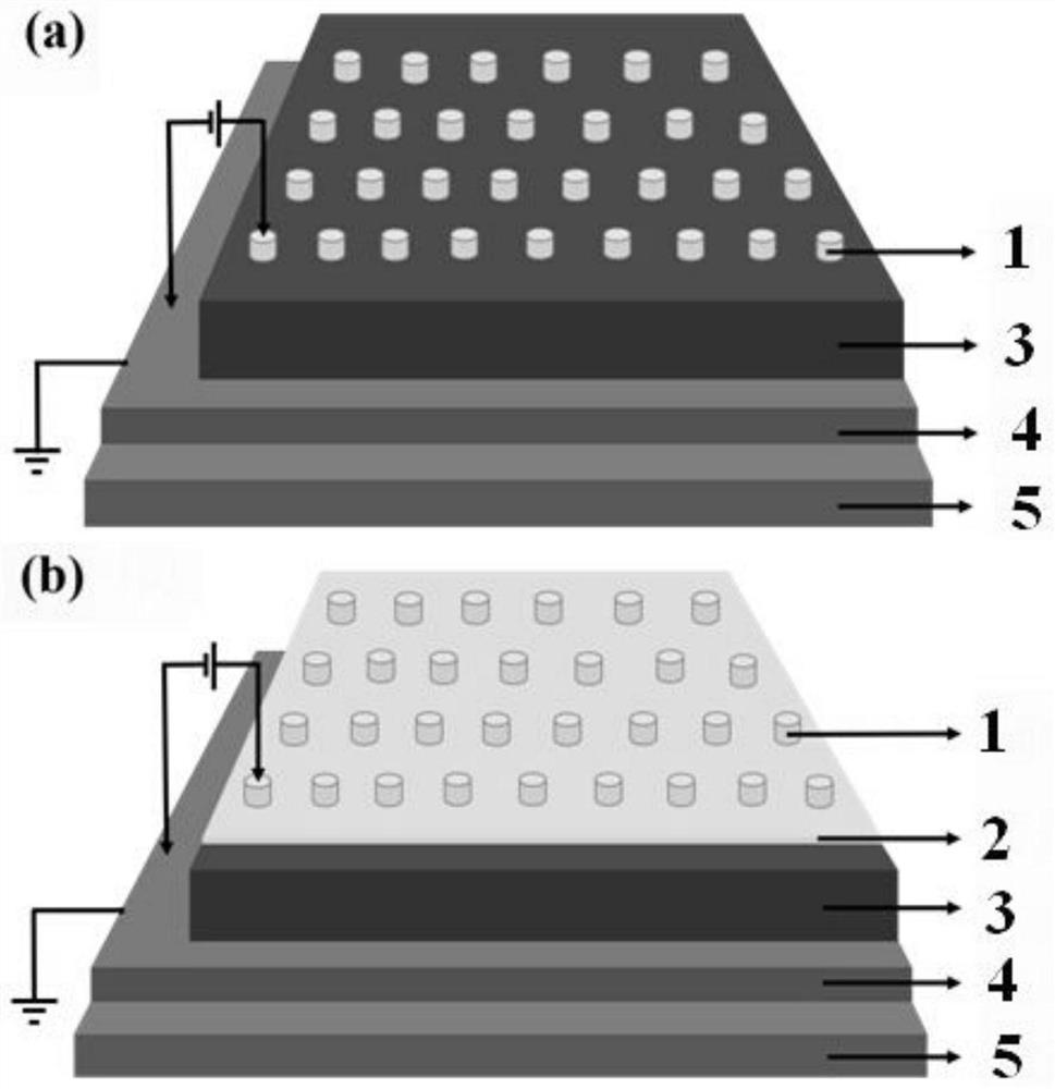
[0038] Prepare a top electrode 1 (the material is Ag, the shape is circular, the thickness is 150nm, the diameter is 300μm), Cs 3 Sb 2 I 9 Perovskite resistive layer 3 (square shape, thickness 270nm, side length 1.7cm), bottom electrode 4 (material is transparent conductive glass indium tin oxide (ITO), square shape, thickness 200nm, side length 1.7cm) and a glass substrate to form the resistive memory of lead-free cesium antimony iodine perovskite, comprising the following steps:

[0039] (1) Pretreatment of the bottom electrode (ITO) deposited on the glass substrate: the bottom electrode (ITO) deposited on the polished surface of the glass substrate (5) by magnetron sputtering is washed with detergent, Deionized water, acetone, and absolute ethanol were sonicated for 20 minutes and then dried.

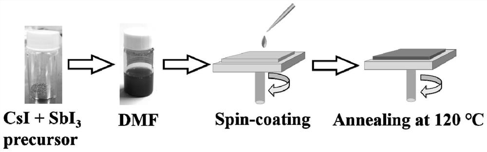
[0040] (2) if figure 1 The procedure shown for the preparation of Cs 3 Sb 2 I 9 Perovskite resistance switch layer: 0.75mmol cesium iodide (CsI) and 0.5mmol antimony iodide (S...

Embodiment 2

[0044] Prepare a top electrode 1 (made of Ag, circular in shape, 150 nm in thickness, and 300 μm in diameter), organic passivation layer 2 (made of polymethyl methacrylate, square in shape, Thickness is 10nm, side length is 1.7cm), Cs 3 Sb 2 I 9 Perovskite resistive layer 3 (square shape, thickness 270nm, side length 1.7cm), bottom electrode 4 (material is transparent conductive glass indium tin oxide (ITO), square shape, thickness 200nm, side length 1.7cm) and glass substrate composed of lead-free cesium antimony iodine perovskite resistive memory, its structure is as figure 2 As shown in b, the resistive memory consists of top electrode, organic passivation layer, Cs 3 Sb 2 I 9 The perovskite resistive layer and the bottom electrode are composed of the following steps:

[0045] (1) Pretreatment of the bottom electrode (ITO) deposited on the glass substrate: the bottom electrode (ITO) deposited on the polished surface of the glass substrate (5) by magnetron sputtering ...


PUM

PropertyMeasurementUnit
thicknessaaaaaaaaaa
thicknessaaaaaaaaaa
diameteraaaaaaaaaa

Abstract

The invention relates to a resistive random access memory based on lead-free cesium antimony iodine perovskite and a preparation method thereof, and belongs to the technical field of perovskite resistive random access memories. According to the resistive random access memory based on the lead-free cesium antimony iodine perovskite and the preparation method of the resistive random access memory, the process is simple, and lead is replaced by antimony in the perovskite resistive random access layer, so that the preparation process of a device is green, environment-friendly and low in toxicity; and meanwhile, the prepared lead-free cesium antimony iodine perovskite resistive random access memory is simple in structure, is a nonvolatile memory, has good storage durability, relatively long data retention, excellent stability and repeatability, is low in erasing voltage, and can realize data storage in a low power consumption state. Various defects in the prior art are effectively overcome, and high industrial utilization value is achieved.

Description

technical field [0001] The invention belongs to the technical field of perovskite resistive memory, and relates to a resistive memory based on lead-free cesium antimony iodine perovskite and a preparation method thereof. Background technique [0002] Memory is an important part of modern information technology and the field of artificial intelligence. However, due to the limitations of theory and technology in the traditional floating gate flash memory, the reduction of its key size has greatly reduced the reliability and stability of the device, making it difficult to meet the requirements of the future. The information storage needs of the explosive growth of human society. Resistive memory is characterized by its simple structure, low operating voltage, fast erasing and writing speed, low power consumption, high storage density, strong durability and repeatability, and good compatibility with traditional complementary metal oxide semiconductor (CMOS) processes, etc. Pros...

Claims


Application Information

Patent Timeline
Patent Type & Authority Applications(China)
IPC IPC(8): H01L45/00
CPCH10N70/801H10N70/882H10N70/011
Inventor 王玉婵袁一鸣张文霞戚飞张楠王振张良睿
Owner CHONGQING UNIV OF POSTS & TELECOMM
Why Eureka
Try Eureka