Gallium oxide-two-dimensional P-type Van der Waals tunneling transistor, dual-band photoelectric detector and preparation method

A technology of tunneling transistors and gallium oxide, which is applied in the field of dual-band deep ultraviolet-infrared photodetectors and its preparation, and achieves the effects of simple preparation process, easy array integration, and reduced leakage current

Active Publication Date: 2022-01-25
XIAN UNIV OF POSTS & TELECOMM
View PDF3 Cites 5 Cited by
  • Summary
  • Abstract
  • Description
  • Claims
  • Application Information

AI Technical Summary

Problems solved by technology

[0008] The purpose of the invention is to solve the Ga 2 o 3 Due to the lack of P-type doping, the technical problems of PN junction dual-band photodetection that cannot realize TFET and gate voltage modulation at the same time, a gallium oxide-two-dimensional P-type van der Waals tunneling transistor, a dual-band pho

Method used


Image

  • Gallium oxide-two-dimensional P-type Van der Waals tunneling transistor, dual-band photoelectric detector and preparation method
  • Gallium oxide-two-dimensional P-type Van der Waals tunneling transistor, dual-band photoelectric detector and preparation method
  • Gallium oxide-two-dimensional P-type Van der Waals tunneling transistor, dual-band photoelectric detector and preparation method

Examples


Embodiment 1

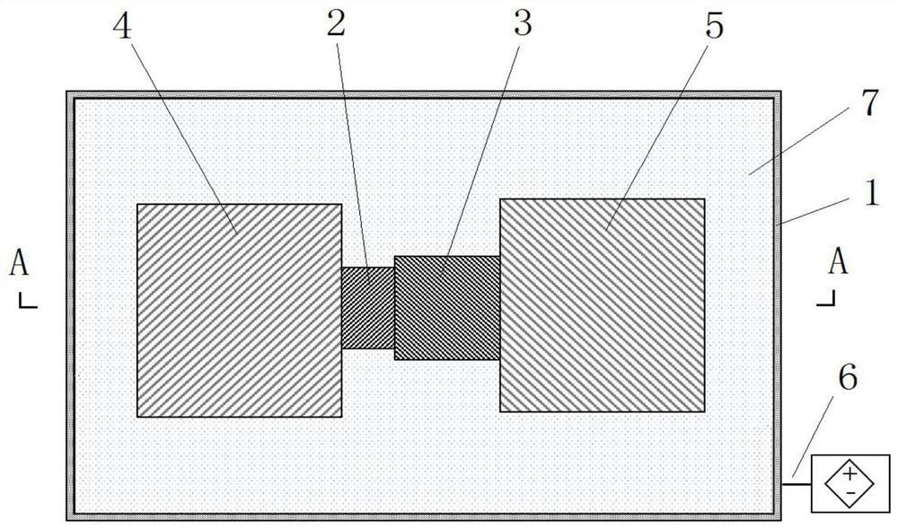
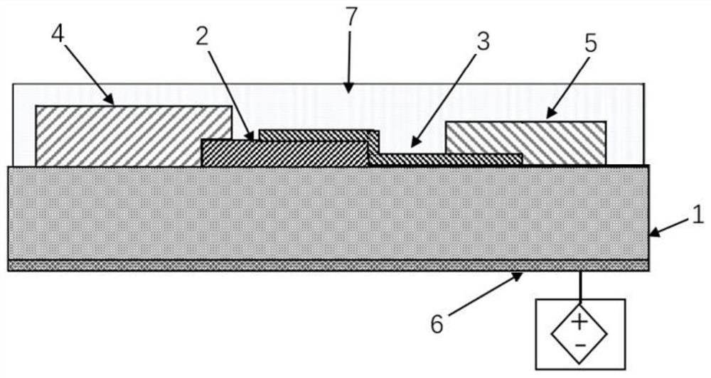
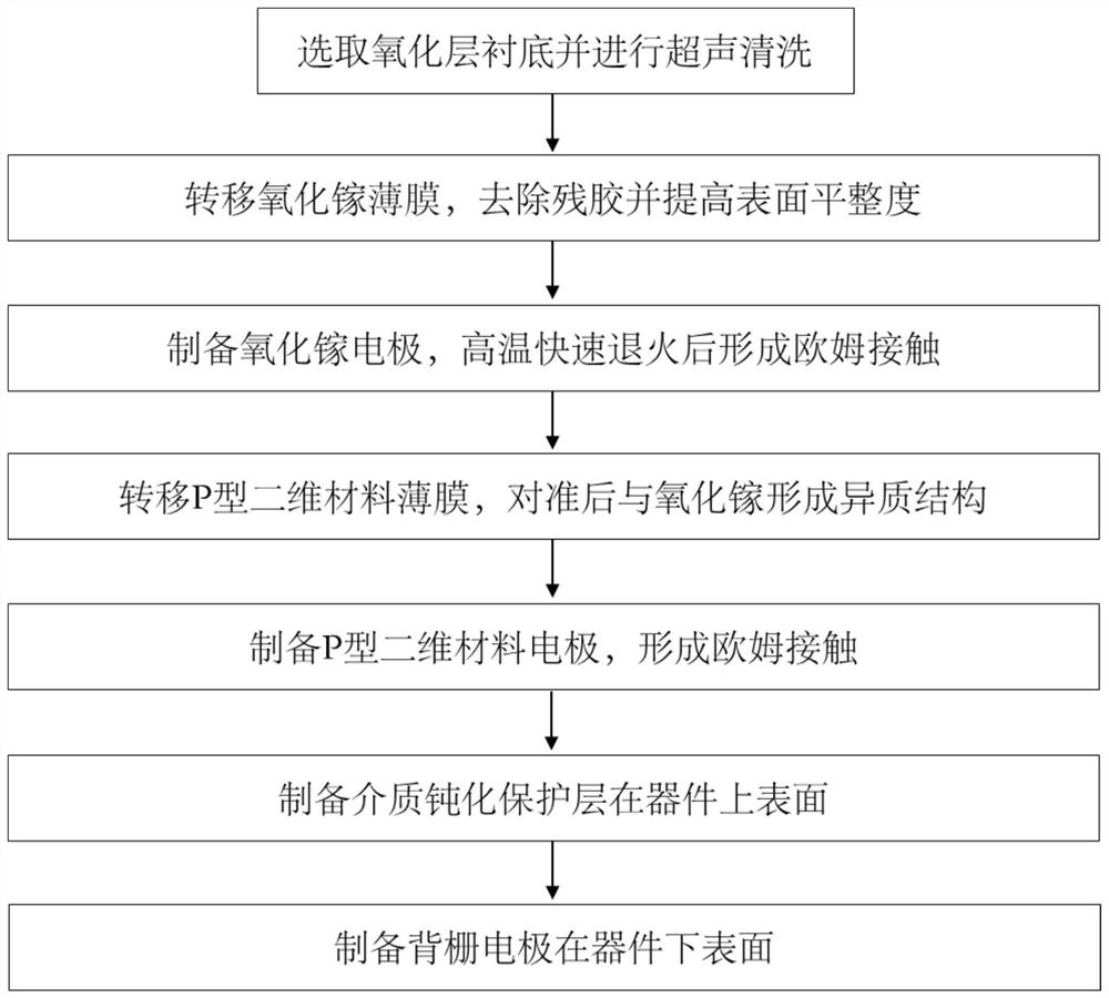
[0084] A gallium oxide-two-dimensional p-type van der Waals tunneling transistor, such as figure 1 , figure 2 As shown, it includes a dielectric oxide layer 1, a dielectric passivation layer 7, a back gate electrode 6, and a transistor unit, wherein the transistor unit includes a gallium oxide layer 2, a P-type two-dimensional material layer 3, a gallium oxide electrode 4, and a P-type two-dimensional material layer. Dimensional material electrode 5. The gallium oxide layer 2 and the P-type two-dimensional material layer 3 are located on the upper surface of the dielectric oxide layer 1; the gallium oxide layer 2 and the P-type two-dimensional material layer 3 form a heterojunction; the gallium oxide layer 2 and the gallium oxide electrode 4, the P-type two-dimensional The three-dimensional material layer 3 and the P-type two-dimensional material electrode 5 respectively form ohmic contacts; the gallium oxide electrode 4 does not contact the P-type two-dimensional material e...

Embodiment 2

[0113] A dual-band photodetection device is implemented in the form of an n×m array, and both n and m are integers greater than or equal to 1. Such as Figure 4 As shown, the array form included in the example is 4×4, and the horizontal and vertical spacing of the array is greater than 20 μm. Of course, other array forms can also be designed, and the larger the array size, the wider the detection area.

[0114] The array type dual-band photodetection device includes a dielectric oxide layer 1 , a back gate electrode 6 , a dielectric passivation layer 7 and transistor units arranged on the upper surface of the dielectric oxide layer 1 .

[0115] The material of dielectric oxide layer 1 is SiO 2 , can also be Al 2 o 3 , HfO 2 , ZrO 2 and other dielectric materials, the lower surface of which is used as a back gate oxide layer; the thickness of the dielectric oxide layer 1 is 30-300nm.

[0116] The transistor unit includes a 4×4 die array, and a gallium oxide electrode 4 and...

Embodiment 3

[0144] Such as Figure 5 As shown, the difference between the present embodiment and the second embodiment is that in order to save wiring and save chip space, in the die array of the transistor unit, the two rows of dies on the left share a P-type two-dimensional material electrode 5 respectively, and the two rows on the right Each row of dies shares a gallium oxide electrode 4 . In other embodiments, it can also be designed that a row of dies share one gallium oxide electrode 4 or one P-type two-dimensional material electrode 5 , of course, other ways of sharing electrodes can also be used if the actual wiring space permits.

[0145] The gallium oxide-two-dimensional P-type van der Waals tunneling transistor provided by the invention and the dual-band photodetection device have a simple preparation process and are easy to realize array integration; by building Ga 2 o3 -P-type two-dimensional (2D) material heterojunction forms a van der Waals energy band structure capable of...


PUM

PropertyMeasurementUnit
Thicknessaaaaaaaaaa
Thicknessaaaaaaaaaa
Thicknessaaaaaaaaaa

Abstract

The invention particularly relates to a gallium oxide-two-dimensional P-type Van der Waals tunneling transistor, a dual-band photoelectric detector and a preparation method, and solves the technical problem that PN junction deep ultraviolet-infrared dual-band detection of the tunneling transistor and gate voltage modulation cannot be realized simultaneously due to lack of P-type doping of Ga2O3 in preparation of an existing UWBG material transistor/photoelectric detector. The transistor and the photoelectric detector comprise a back gate electrode, a dielectric oxide layer, a gallium oxide layer, a gallium oxide electrode forming ohmic contact, a P-type two-dimensional material layer, a P-type two-dimensional material electrode forming ohmic contact, and a dielectric passivation layer. The gallium oxide layer and the P-type two-dimensional material layer are partially overlapped to form a heterojunction; the gallium oxide layer is an unintentionally doped or doped Ga2O3 quasi-two-dimensional crystal film; and the P-type two-dimensional material layer is black phosphorus or a beta-phase tellurium elementary substance or a 2H-phase molybdenum ditelluride or tungsten diselenide or platinum diselenide film. In addition, the invention also provides a preparation method of the transistor and the dual-band photoelectric detector.

Description

technical field [0001] The invention relates to a transistor / photodetector device and a preparation method, in particular to a quasi-two-dimensional gallium oxide (Ga 2 o 3 )-two-dimensional p-type van der Waals tunneling transistor and dual-band deep ultraviolet-infrared (DUV-IR) photodetector and preparation method. Background technique [0002] Gallium oxide has received extensive attention as a novel ultra-wide bandgap (UWBG) semiconductor material, which has a quasi-direct bandgap of 4.6-4.9eV, up to 2×10 7 The electron saturation drift velocity of cm / s, and the photoresponse peak corresponds to the sun-blind band (250-270nm), Ga 2 o 3 It has important application value in the fields of power electronics and solar-blind deep ultraviolet detection. [0003] The preparation of field effect transistor (FET) devices with large switching ratio and steep subthreshold swing (SS) is of great significance for improving the response speed of the device and reducing energy con...

Claims


Application Information

Patent Timeline
IPC IPC(8): H01L29/06H01L29/24H01L29/739H01L31/032H01L31/0352H01L31/101H01L31/112H01L31/18H01L21/34
CPCH01L29/7391H01L29/66969H01L29/0684H01L29/24H01L31/1013H01L31/112H01L31/18H01L31/035209H01L31/032Y02P70/50
Inventor 王湛刘朋源孙静关云鹤刘翔泰陆琴王少青贾一凡陈海峰马晓华
Owner XIAN UNIV OF POSTS & TELECOMM
Why Eureka
Try Eureka