Double-groove silicon carbide MOSFET structure and manufacturing method

A silicon carbide and double-groove technology, which is applied in semiconductor/solid-state device manufacturing, electrical components, circuits, etc., can solve problems such as limiting operating frequency and system efficiency, serious electric field concentration effect, and increased on-resistance, and achieves improved Reliability, reduced peak field strength, reduced on-resistance effects

Active Publication Date: 2022-02-01
北京昕感科技有限责任公司
View PDF4 Cites 6 Cited by
  • Summary
  • Abstract
  • Description
  • Claims
  • Application Information

AI Technical Summary

Problems solved by technology

These two methods can achieve the transfer of the peak position of the field intensity, but both will compress the path width of the current flowing from the channel to the drift layer, resulting in an increase in the on-resistance
The double-trench silicon carbide MOSFET structure proposed by Rohm can achieve a good compromise between the critical breakdown voltage and on-resistance, but the electric field concentration effect at the middle of the bottom of the gate trench is still serious, and the gate-drain capacitance Higher, which limits the improvement of operating frequency and system efficiency

Method used


Image

  • Double-groove silicon carbide MOSFET structure and manufacturing method
  • Double-groove silicon carbide MOSFET structure and manufacturing method
  • Double-groove silicon carbide MOSFET structure and manufacturing method

Examples


Embodiment Construction

[0023] Embodiments of the present invention are described in detail below, examples of which are shown in the drawings, wherein the same or similar reference numerals designate the same or similar elements or elements having the same or similar functions throughout. The embodiments described below by referring to the figures are exemplary only for explaining the present invention and should not be construed as limiting the present invention.

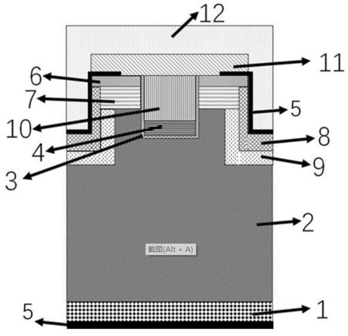
[0024] see figure 1 , the present invention discloses a double-trench silicon carbide MOSFET structure (hereinafter referred to as the structure), which is composed of a plurality of cell arrangements, each cell has an N++ type substrate 1 and an N-type drift layer 2, and in the N-type drift A gate trench and a source trench are formed on layer 2; an N-type hole blocking layer 9 and a P+ type shielding layer 8 are sequentially formed around the source trench from bottom to top, and the height of the N-type hole blocking layer 9 is not lo...


PUM

PropertyMeasurementUnit
thicknessaaaaaaaaaa

Abstract

The invention discloses a double-groove silicon carbide MOSFET structure and a manufacturing method. The structure is formed by arranging a plurality of cells, wherein each cell is provided with a substrate and a drift layer; each drift layer is provided with a gate trench and a source trench, an N-type hole barrier layer and a P+ type shielding layer are arranged around the source trench, and source metal is formed in the source trench; a P- type base region is formed at the tops of each drift layer and each N-type hole blocking layer, N+ type source regions are formed at the tops of the P- type base regions and the P+ type shielding layers, and ohmic contact metal layers are arranged between the N+ type source regions and source electrode metal; gate thermal oxidation dielectric layers are formed on the bottom surfaces, the inner side surfaces and the like of the gate trenchs, the gate thermal oxidation dielectric layers are cavity-shaped, and gate precipitation dielectric layers and gate electrodes are formed in the cavities; and interlayer mediums are arranged between the gate electrodes and the source electrode metal. According to the above structure, the reliability of a gate dielectric layer of the device can be improved, and on-resistance is reduced, so on-static loss is reduced, gate-drain capacitance and gate charge are reduced, and the dynamic loss of a switch is reduced.

Description

technical field [0001] The invention relates to the field of semiconductors, in particular to a double-groove silicon carbide MOSFET structure and a manufacturing method. Background technique [0002] Silicon carbide is a third-generation semiconductor material. Compared with the first-generation semiconductor material silicon, it has a larger band gap, a larger critical breakdown field strength, a faster electron saturation drift speed, and a higher heat dissipation. Conductivity. Therefore, silicon carbide power semiconductor devices, especially silicon carbide MOSFETs, can work better under high temperature, high pressure, and high frequency conditions, significantly improving the energy efficiency of power electronic systems, improving system heat dissipation, and reducing system volume. [0003] A key challenge for SiC MOSFETs is the existence of interface states at the SiC / SiO2 interface and the scattering effect of trapped charges on electrons, resulting in lower cha...

Claims


Application Information

Patent Timeline
Patent Type & Authority Applications(China)
IPC IPC(8): H01L29/06H01L29/423H01L29/78H01L21/28H01L21/336
CPCH01L29/7827H01L29/66068H01L29/0696H01L29/0684H01L29/401H01L29/4236H01L29/42364
Inventor 张文渊马鸿铭王哲
Owner 北京昕感科技有限责任公司
Why Eureka
Try Eureka