
High-efficiency stable large-area semitransparent perovskite solar cell and preparation method thereof
A solar cell and perovskite technology, applied in semiconductor/solid-state device manufacturing, circuits, photovoltaic power generation, etc., can solve the problems of low power conversion efficiency, low power conversion efficiency, small active area, etc., to improve battery performance and repeatability properties, reduce defects and losses, and smooth the surface of the film
- Summary
- Abstract
- Description
- Claims
- Application Information
AI Technical Summary
Problems solved by technology
Method used
Image

Examples
Embodiment 1
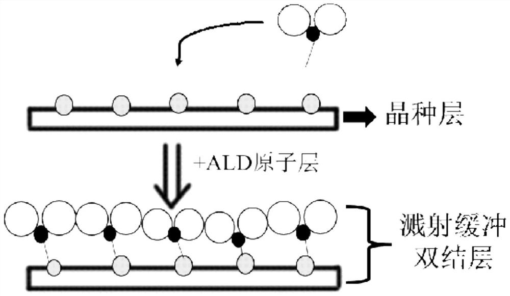
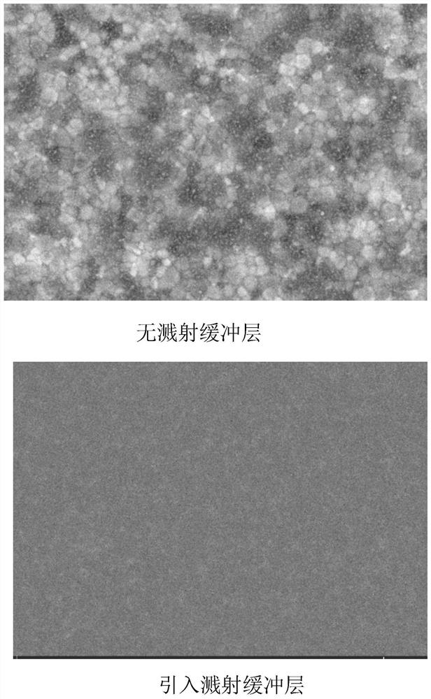
[0039] refer to Figure 4 , is a kind of highly efficient and stable large-area translucent perovskite solar cell disclosed in the present application, comprising a conductive substrate layer 1, and a hole transport layer 2 is formed on the surface of the conductive substrate layer 1 after laser scribing treatment; A perovskite light-absorbing layer 3 is formed on the surface of the hole transport layer 2; an electron transport layer 4 is formed on the surface of the perovskite light-absorbing layer 3; a sputtering buffer double layer 5 is formed on the surface of the electron transport layer 4; the sputtering buffer double layer 5 includes a The seed layer 50 formed on the surface of the electron transport layer 4 by the solution method and the ALD atomic layer 6 formed on the surface of the seed layer 50 through the self-limiting chemical reaction of the atomic layer deposition precursor and the co-reactant; on the sputtering buffer double layer 5 The perovskite light-absorb...
Embodiment 2
[0056] The difference between embodiment 2 and embodiment 1 is:
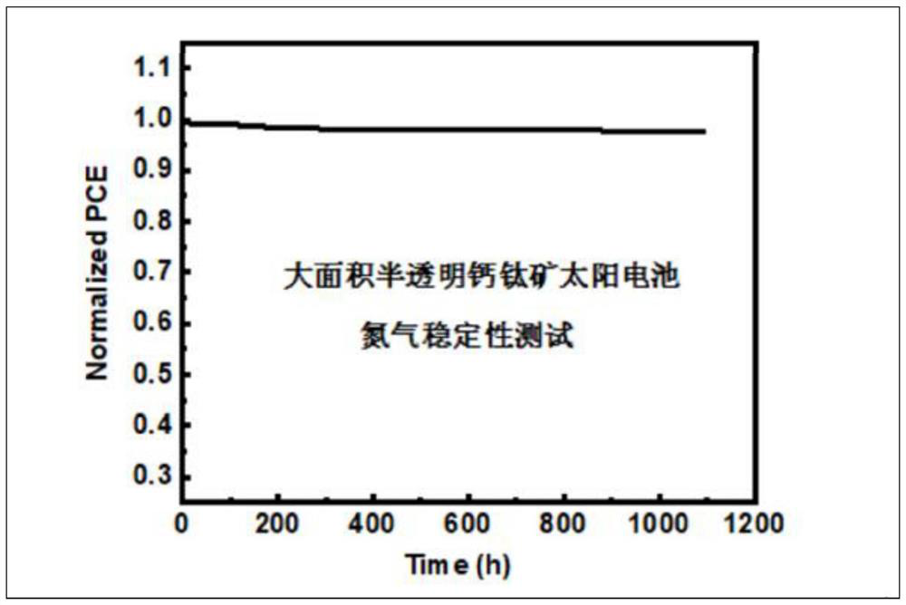
[0057] A method for preparing an efficient and stable large-area translucent perovskite solar cell, the preparation of a large-area translucent perovskite solar cell with a substrate size of 5.7*5.7 square centimeters, such as Figure 4 Schematic diagram of the structure of a large-area semitransparent perovskite solar cell shown in the cell, Figure 5 and Figure 6 They are the area measurement diagram and the actual effect diagram of the large-area translucent perovskite solar cell, including the following steps:
[0058] (1) Clean the substrate
[0059] The transparent conductive glass ITO (indium tin oxide) was ultrasonically cleaned by a mixed solution prepared by hellmanex III cleaning solution and deionized water at a ratio of 1:20, deionized water, ethanol, and isopropanol for 15 minutes, then dried, and then subjected to oxygen plasma After processing for 10 minutes, the ITO glass substrate layer is ...
PUM
| Property | Measurement | Unit |
|---|---|---|
| thickness | aaaaa | aaaaa |
| thickness | aaaaa | aaaaa |
Abstract
Description
Claims
Application Information