Silicon carbide MOSFET device with integrated diode and manufacturing method

A technology of silicon carbide and diodes, which is applied in the field of trench silicon carbide MOSFET device structure, can solve the problems of poor temperature characteristics of Schottky interface, dependence of reverse characteristics on width ratio, influence of device forward characteristics, etc., to achieve improved oxidation layer reliability, save chip area, and improve the effect of current density

Pending Publication Date: 2022-03-01
UNIV OF ELECTRONICS SCI & TECH OF CHINA
View PDF7 Cites 12 Cited by
  • Summary
  • Abstract
  • Description
  • Claims
  • Application Information

AI Technical Summary

Problems solved by technology

Since the barrier height of the Schottky contact is lower than that of the ohmic contact, the on-chip integrated Schottky diode can effectively reduce the turn-on voltage of the device, but its reverse characteristics strongly depend on the width of the P+ region and the N+ region Proportion
When the ratio of the width of the P+ region is small, the leakage current of the device increases, the breakdown voltage decreases sharply, and the surge current capability is poor; when the ratio of the width of the P+ region is large, the forward characteristics of the device will be seriously affected
At the same time, the temperature characteristics of the Schottky interface in the junction barrier Schottky diode are poor, resulting in a sharp increase in the leakage current of the device at high temperature

Method used


Image

  • Silicon carbide MOSFET device with integrated diode and manufacturing method
  • Silicon carbide MOSFET device with integrated diode and manufacturing method
  • Silicon carbide MOSFET device with integrated diode and manufacturing method

Examples


Embodiment Construction

[0031] Embodiments of the present invention are described below through specific examples, and those skilled in the art can easily understand other advantages and effects of the present invention from the content disclosed in this specification. The present invention can also be implemented or applied through other different specific implementation modes, and various modifications or changes can be made to the details in this specification based on different viewpoints and applications without departing from the spirit of the present invention.

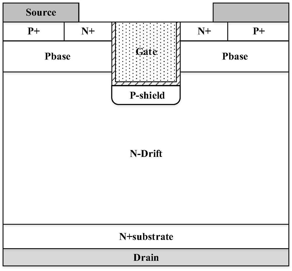
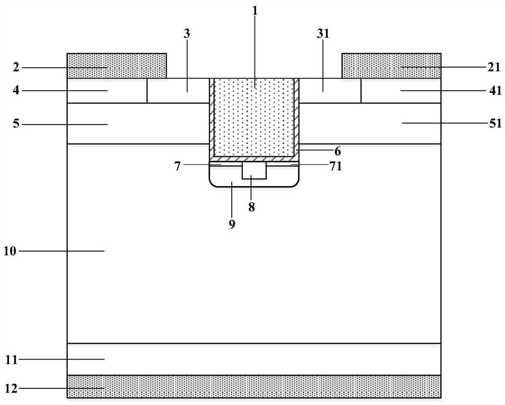
[0032] Such as figure 2As shown, a trench type silicon carbide MOSFET device integrating a low conduction voltage drop diode, including an N+ substrate 11, an N-drift region 10 above the N+ substrate 11; an upper part of the N-drift region 10 A P-type shielding layer 9 is provided, a shielding layer N+ source region 8 is arranged above the P-type shielding layer 9, and a first N-type channel region 7 and a second N-type channel regio...


PUM


Abstract

The invention provides a silicon carbide MOSFET (Metal-Oxide-Semiconductor Field Effect Transistor) device with an integrated diode and a manufacturing method. The device comprises a source ohmic contact region, a drain ohmic contact region, an N + substrate, an N-drift region, a P-type base region, a P + source region, an N + source region, a P-type shielding layer, a shielding layer N + source region, an N-type channel region, a gate dielectric layer and a polysilicon gate. According to the trench type silicon carbide MOSFET device provided by the invention, the chip area is greatly saved in a mode of integrating the diodes in the chip. The N-type channel region is introduced to the bottom of the trench, so that the electron barrier height at the interface of the oxide layer is adjusted, the third quadrant characteristic of the device is remarkably improved, the low third quadrant turn-on voltage is realized, and the bipolar degradation effect is avoided; multiple channels are connected in parallel, so that the forward current capability of the device is improved, and the on-resistance is reduced; and the P-type shielding layer wraps and protects the gate groove, so that the electric field of the gate oxide layer is reduced, and the reliability of the device oxide layer is enhanced.

Description

technical field [0001] The invention belongs to the technical field of power semiconductors, and in particular relates to a trench silicon carbide MOSFET device structure integrating low conduction voltage drop diodes. Background technique [0002] As one of the representatives of the third-generation wide bandgap semiconductor materials, silicon carbide (Silicon Carbide) material has a large bandgap (3.26eV), a high critical breakdown electric field (3MV / cm), and a high thermal conductivity (490W / Mk ) and high electron saturation drift velocity (2×10 7 cm / s) and other characteristics, it has broad application prospects in the fields of high-power, high-temperature and high-frequency power electronics. [0003] As the most widely used unipolar device in silicon carbide power devices, silicon carbide MOSFET has low switching loss and high switching frequency, and is more suitable for high frequency working conditions, coupled with its extremely low on-resistance and excellen...

Claims


Application Information

Patent Timeline
Patent Type & Authority Applications(China)
IPC IPC(8): H01L29/78H01L29/06H01L27/07H01L21/336
CPCH01L29/0638H01L29/7827H01L27/0727H01L29/66666
Inventor 邓小川邢云鹏李松俊李旭李轩张波
Owner UNIV OF ELECTRONICS SCI & TECH OF CHINA
Why Eureka
Try Eureka