SiC-based junction field effect transistor and manufacturing method thereof

A technology of field effect transistors and junctions, which is applied in semiconductor/solid-state device manufacturing, electrical components, circuits, etc., can solve problems such as low breakdown voltage, high on-resistance, and operating temperature limitations, and achieve large band gap, Effect of high intrinsic temperature and small pinch-off voltage

Pending Publication Date: 2022-03-22
XI'AN UNIVERSITY OF ARCHITECTURE AND TECHNOLOGY
View PDF0 Cites 0 Cited by
  • Summary
  • Abstract
  • Description
  • Claims
  • Application Information

AI Technical Summary

Problems solved by technology

[0004] The purpose of the present invention is to solve the problems of the above-mentioned junction field effect transistors, and propose a SiC-based junction field effect transistor and its manufacturing method, which are used to solve the problems of high on-resistance, low breakdown voltage, and working temperature restrictions. technical problem

Method used


Image

  • SiC-based junction field effect transistor and manufacturing method thereof
  • SiC-based junction field effect transistor and manufacturing method thereof
  • SiC-based junction field effect transistor and manufacturing method thereof

Examples


Embodiment 1

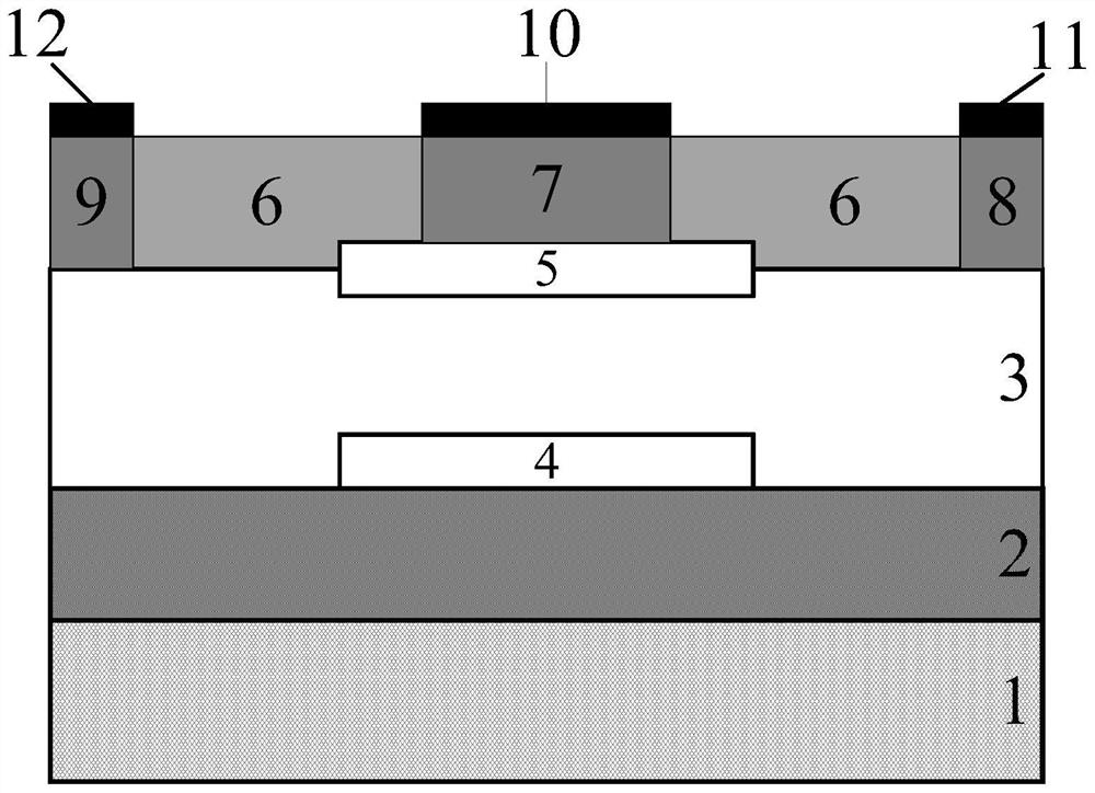
[0029] Example 1: Refer to figure 1 , The SiC-based junction field effect tube proposed by the present invention is discharged from silicon carbide as a substrate, and the silicon carbide substrate 1 is discharged from the silicon carbide epitaxial layer 2, the first P-type doped region 4, the second P-type doped region 5, two p-type doped regions are provided with n-type doped regions 3;

[0030] The intermediate position of the n-type doped region 3 is adjacent to the lower surface and the upper surface, respectively, as a first p-doped region 4 as a back gate, respectively, a second P-type doped region 5 as a normal gate; N-type doped The silica insulating layer 6, the ohmic contact layer 7, the source contact layer 8 and the drain contact layer 9 are formed in the upper surface of the region 3; wherein the silica insulating layer 6 is divided into two parts, and a portion is located in the ohmic contact layer 7 and the source. Between the contact layer 8, the other portion is ...

Embodiment 2

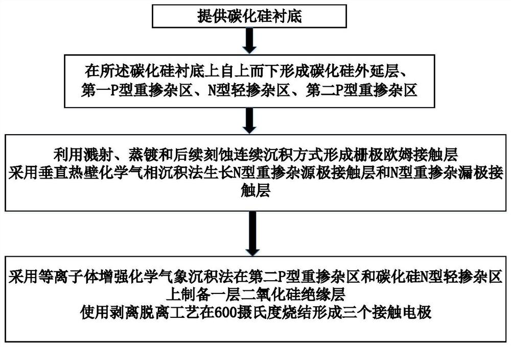
[0036] Example 2: Reference figure 1 and figure 2 , The specific steps are as follows: The specific steps are as follows:

[0037] Step 1) Provide a heavily doped silicon carbide substrate;

[0038] Step 2) Grow the silicon carbide epitaxial layer on the silicon carbide substrate;

[0039] Step 3) Plasma doping in the center portion of the silicon carbide epitaxial layer, forming a first P-type doped region, and its carrier concentration ranges from 1 × 10 18 cm -3~ 1 × 10 19 cm -3 ;

[0040] Step 4) An n-type silicon carbide is prepared on the silicon carbide epitaxial layer and the first P-type doped region, and the desired doped pattern is obtained on the N-shaped silicon carbide; the carrier concentration range of n-type silicon carbide 1.5 × 10 17 cm -3~ 2 × 10 17 cm -3 ;

[0041] Step 5) Plasma doping in the position of the N-type silicon carbide after the photolithography, plasma doping, forming a second P-type doped region, and its carrier concentration ranges from 1 × 10 ...

Embodiment 3

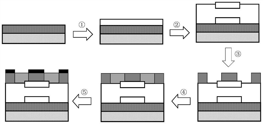
[0045] Example 3: Reference image 3 The overall step of the present embodiment is based on the second embodiment, and gives a specific parameter and process operation further describe the implementation steps of the method of the present invention:

[0046] Step 1: Select the substrate.

[0047] First, 250 nm P-type doped silicon carbide is first used as the initial material, which is used as a substrate.

[0048] Step 2: Grow the epitaxial layer.

[0049] The epitaxial growth technique was used to grow 200 nm P-type silicon carbide epitaxial layer in the substrate in the substrate using a vertical thermal wall chemical vapor deposition method.

[0050] Step 3: Growing silicon carbide first P-type retaining region.

[0051] The chemical vapor deposition method CVD growth of 50 nm of silicon carbide P-type retaining region is grown on silicon carbide epitaxial layer; image 3 The process flow 1 is shown.

[0052] Step 4: Growing silicon carbide n-type lightly doped regions.

[0053]...


PUM


Abstract

The invention discloses a SiC-based junction field effect transistor and a manufacturing method thereof, and mainly solves the problems of high on resistance, low breakdown voltage and working temperature limitation of the existing device. Comprising a silicon carbide substrate, a silicon carbide epitaxial layer located above the substrate, and an N-type doped region on the upper surface of the epitaxial layer as a channel; a first P-type doped region serving as a back gate is arranged between the N-type doped region and the silicon carbide epitaxial layer, and a second P-type doped region serving as a positive gate is arranged on the upper surface of the N-type doped region; forming a source electrode contact layer and a drain electrode contact layer on the surface of the N-type doped region by adopting a vertical hot wall chemical vapor deposition method, forming an ohmic contact layer on the surface of the second P-type doped region, and arranging a contact electrode on the ohmic contact layer; and electrical isolation is formed among the gate metal electrode, the source metal electrode and the drain metal electrode by using the insulating layer. According to the invention, the current conduction capability and the working voltage range can be improved while a relatively small pinch-off voltage is maintained, and the device is simple in structure and easy to prepare and has the characteristic of high temperature resistance.

Description

Technical field [0001] The present invention belongs to the technical field of semiconductor devices, and further relates to a junction field effect device, specifically a SiC-based junction field effect tube and a manufacturing method thereof, can be used to make power devices, digital logic circuit devices or power electronic devices. Background technique [0002] Fielding effect tube is a voltage amplifier device having three electrodes: source, gate and drain. Field effect transistors, also known as single-pole type transistors, is a semiconductor device that controls output loop currents using an electric field effect of an input loop, typically divided into junction and metal oxide semiconductor type. The junction field effect tube JFET is one of the most common semiconductor devices, and there are two types of n-type and p-type, most commonly used by N-channel JFETs. The junction field effect tube has a small size, low frequency noise small and input impedance, and has bro...

Claims


Application Information

Patent Timeline
Patent Type & Authority Applications(China)
IPC IPC(8): H01L29/808H01L29/16H01L21/337
CPCH01L29/808H01L29/1608H01L29/66068
Inventor 樊庆扬赵睿达赵颖博陈帅铭吴杰
Owner XI'AN UNIVERSITY OF ARCHITECTURE AND TECHNOLOGY
Why Eureka
Try Eureka