VO2-based multi-layer thin film structure and preparation method of VO2-based multi-layer thin film structure product
A thin film structure, VO2 technology, applied in the field of spacecraft thermal control, can solve the problems of complex structure and preparation process, high energy consumption, expensive manufacturing and emission costs, etc., achieve high visible light transmittance, low solar absorption rate, good Effects of thermal control properties and thermal shock resistance
- Summary
- Abstract
- Description
- Claims
- Application Information
AI Technical Summary
Problems solved by technology
Method used
Image
Examples
Embodiment 1
[0100] In this example, the JGP450 magnetron sputtering deposition system was used to prepare VO 2 Multilayer film structure. In the experiment, with the (100) direction single crystal silicon wafer as the substrate, high-purity metal targets titanium target (purity 99.99%), high-purity metal silver target (purity 99.99%), high-purity metal aluminum target (purity 99.999%) and a high-purity metal vanadium target (purity 99.9%) to prepare a multilayer film structure. Ag / Al 2 o 3 / VO 2 The preparation process steps of the thin-film structure SRD device include: (1) radio frequency sputtering deposition transition layer Ti thin film; (2) DC sputtering deposition reflection layer Ag thin film; (3) DC reactive sputtering deposition optical dielectric layer Al 2 o 3 thin film; (4) DC reactive sputtering deposition of functional layer VO 2 Film; (5) VO 2 Subsequent heat treatment of the film. Among them, the specific experimental process of preparing thin films by magnetron s...
experiment example 1
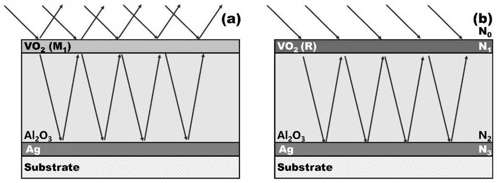
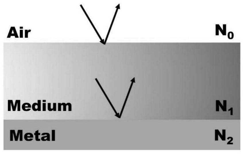
[0118] After confirming that the thin-film structure is an F-P resonant cavity, it is necessary to find a suitable thin-film material as the optical dielectric layer. By changing the material of the optical dielectric layer, the Al 2 o 3 , SiO 2 、TiO 2 and HfO 2 The effect of optical dielectric materials on the thermal control performance of SRD devices. According to the previous derivation, the thickness of the optical medium layer of the F-P resonator cavity and the designed specific wavelength band should satisfy λ / 4n, which is the optical thickness (qw). The thickness is designed for a wavelength of 10 μm, and the thickness parameter selection of various materials is shown in Table 2. Image 6 It is the influence of different optical dielectric materials on the infrared absorption rate of SRD devices. It can be seen that for the F-P resonator, different optical dielectric materials have no obvious influence on the infrared absorption performance of SRD. However, in ...
experiment example 2
[0122] When Al 2 o 3 After the material is selected as the optical medium layer, the thickness of the optical medium layer needs to be determined. selected VO 2 Functional layer thickness (50nm), respectively simulated 900nm, 1200nm, 1500nm, 1700nm thickness Al 2 o 3 The effect of thin films on the infrared absorption ability of SRD devices. Figure 7 Infrared absorptivity of SRD device varies with Al 2 o 3 Layer thickness variation curve. It can be seen that Al 2 o 3 The thickness of the film determines the position of the absorption peak of the F-P resonator. Al 2 o 3 The thickness of the layer can adjust the propagation phase of the light wave in the film structure, and achieve coherent extinction for the light beam satisfying the wavelength band of λ / 4n optical thickness. It can be seen that when Al 2 o 3 When the thickness of the layer increases, the position of the absorption peak of the device at high temperature moves to the long-wave direction, and the a...
PUM
| Property | Measurement | Unit |
|---|---|---|
| thickness | aaaaa | aaaaa |
| thickness | aaaaa | aaaaa |
| thickness | aaaaa | aaaaa |
Abstract
Description
Claims
Application Information


