Gallium nitride Schottky barrier diode with vertical structure and manufacturing method thereof

A Schottky potential and vertical structure technology, which is applied in semiconductor/solid-state device manufacturing, electrical components, circuits, etc., can solve problems such as high current path resistance, difficult to obtain high current devices, complex manufacturing process, etc., and achieve leakage current Effect of small size, few defects, and low leakage current

Pending Publication Date: 2022-04-08
江西誉鸿锦材料科技有限公司
View PDF0 Cites 0 Cited by
  • Summary
  • Abstract
  • Description
  • Claims
  • Application Information

AI Technical Summary

Problems solved by technology

[0003] A Schottky barrier diode with a lateral structure made of a GaN layer is formed on a sapphire substrate. Both the ohmic electrode and the Schottky barrier electrode are arranged on the surface of the device, and the current also flows in a lateral direction parallel to the substrate surface. , its manufacturing process is complicated, the resistance of the current path is large, and it is difficult to obtain a device with a large current

Method used


Image

  • Gallium nitride Schottky barrier diode with vertical structure and manufacturing method thereof
  • Gallium nitride Schottky barrier diode with vertical structure and manufacturing method thereof

Examples


Embodiment 1

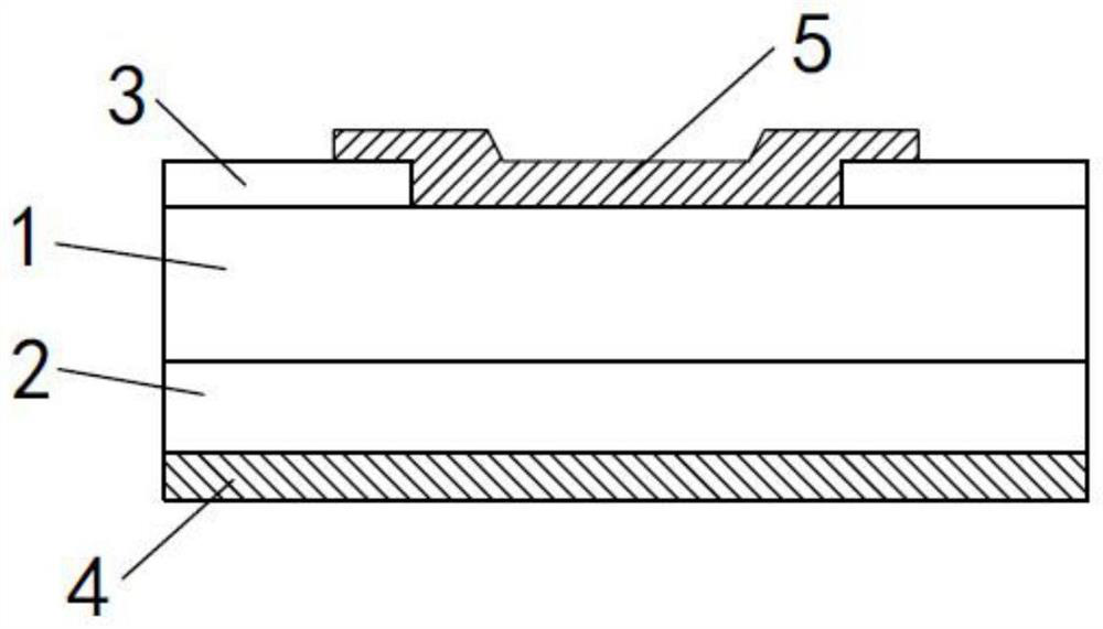
[0046] the n - -GaN layer 1 is n - -GaN substrate layer, the n + -GaN layer 2 is n + - GaN epitaxial layer.

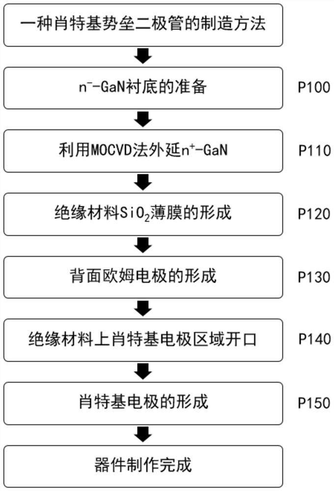
[0047] The fabrication method of the gallium nitride Schottky barrier diode with vertical structure specifically includes the following steps:

[0048] P100:n - -GaN substrate preparation

[0049] 2 inches in diameter, 430 microns thick, (0001) surface, mirror polished n on both sides - -GaN single crystal is used as the substrate layer, and the impurity concentration is 1×10 16 cm -3 , the carrier mobility is at 650cm 2 / VS.

[0050] P110: Epitaxy n by MOCVD + -GaN

[0051] First, the two mirror-polished n - -GaN substrate layer 1 is put into the reaction furnace of MOCVD equipment, in the reaction furnace of MOCVD equipment, import hydrogen (H 2 ) and nitrogen (N 2 ), the flow ratio of hydrogen gas and nitrogen gas can be set in the range of 10:(10~0), heat the substrate to 1100°C and keep it warm for 5~10 minutes, for n - - The surface of the GaN subs...

Embodiment 2

[0075] the n - -GaN layer 1 is n - -GaN epitaxial layer, the n + -GaN layer 2 is n + -GaN substrate layer.

[0076] The fabrication method of the gallium nitride Schottky barrier diode with vertical structure specifically includes the following steps:

[0077] Present embodiment adopts diameter 2 inches, thickness 325 microns, (0001) face, the n of two-sided mirror polishing + -GaN single crystal is used as the substrate layer, and the impurity concentration is 2×10 18 cm -3 , the carrier mobility is at 500cm 2 / VS.

[0078] First, the two mirror-polished n + -GaN single crystal substrate is placed in the reaction furnace of MOCVD equipment, and hydrogen gas (H 2 ) and nitrogen (N 2 ), the flow ratio of hydrogen gas and nitrogen gas can be set in the range of 10:(10~0), heat the substrate to 1100°C and keep it warm for 5~10 minutes, for n + -The surface of the GaN substrate is cleaned at high temperature.

[0079] Then, put n + -The temperature of the GaN substrat...


PUM

PropertyMeasurementUnit
Thicknessaaaaaaaaaa
Thicknessaaaaaaaaaa
Thicknessaaaaaaaaaa

Abstract

The invention discloses a gallium nitride Schottky barrier diode with a vertical structure and a manufacturing method thereof, the gallium nitride Schottky barrier diode comprises an n-GaN layer (1), the upper surface of the n-GaN layer (1) is provided with an insulating protection layer (3) and a Schottky barrier electrode (5), and the lower surface of the n-GaN layer (1) is sequentially provided with an n +-GaN layer (2) and an ohmic electrode (4) from top to bottom; the insulating protection layer (3) is arranged on a part of the upper surface of the n-GaN layer (1), the Schottky barrier electrode (5) is arranged in a region, which is not provided with the insulating protection layer (3), of the upper surface of the n-GaN layer (1), and the edge of the Schottky barrier electrode (5) covers the insulating protection layer (3) to form a field plate structure. The Schottky barrier diode of the vertical structure is made of GaN materials, the GaN materials have the advantages of being wide in band gap, high in breakdown electric field intensity, high in electron mobility, high in electron saturation speed and the like, the problems that the Schottky barrier diode is large in current, high in reverse voltage and the like are solved, and large current, high voltage resistance and miniaturization of the diode are achieved.

Description

technical field [0001] The invention relates to the technical field of semiconductors, in particular to a gallium nitride Schottky barrier diode with a vertical structure and a manufacturing method thereof. Background technique [0002] Schottky barrier diodes (SBDs) are widely used in various power supply systems, automobiles, and standard power modules as rectification or switching devices. The general requirements for Schottky barrier diodes are large forward current density, small reverse leakage current, high reverse withstand voltage, ability to work under high power or high frequency conditions, long life, good stability, and low cost. [0003] A Schottky barrier diode with a lateral structure made of a GaN layer is formed on a sapphire substrate. Both the ohmic electrode and the Schottky barrier electrode are arranged on the surface of the device, and the current also flows in a lateral direction parallel to the substrate surface. , its manufacturing process is comp...

Claims


Application Information

Patent Timeline
IPC IPC(8): H01L29/872H01L29/20H01L29/40H01L21/329
Inventor 邵春林闫怀宝闫发旺
Owner 江西誉鸿锦材料科技有限公司
Why Eureka
Try Eureka