
Method for preparing hafnium oxide film by chemical liquid phase deposition method

A chemical liquid deposition, hafnium oxide technology, applied in liquid chemical plating, metal material coating process, coating and other directions, can solve the problem of no reports, and achieve low cost, good leakage, high transmittance. Effect

Active Publication Date: 2022-04-29
FUZHOU UNIV
View PDF3 Cites 0 Cited by
  • Summary
  • Abstract
  • Description
  • Claims
  • Application Information

AI Technical Summary

Problems solved by technology

Someone has used the chemical liquid phase deposition method to prepare silicon oxide films before, and this method has been applied to the preparation of many metal oxide films, such as titanium oxide, iron oxide, zinc oxide, etc. Preparation of high quality HfO 2 Film studies have not been reported

Method used

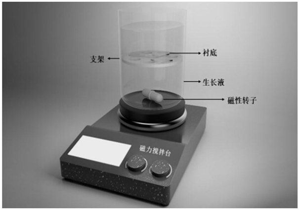
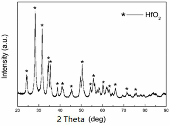

Image

  • Method for preparing hafnium oxide film by chemical liquid phase deposition method
  • Method for preparing hafnium oxide film by chemical liquid phase deposition method
  • Method for preparing hafnium oxide film by chemical liquid phase deposition method

Examples


Embodiment 1

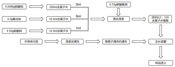
[0042] A method for preparing a hafnium oxide thin film by chemical liquid phase deposition, comprising the following steps:

[0043] (1) Put the indium phosphide substrate into acetone and ultrasonically clean it for 15 minutes, then put it in absolute ethanol for 15 minutes, then put it into deionized water and ultrasonically clean it for 15 minutes, and blow dry it with nitrogen after taking it out;

[0044] (2) Put the cleaned indium phosphide substrate into a plasma cleaning machine for cleaning, set the working voltage to 625V, set the working current to 10mA, and set the time to 10min;

[0045] (3) Weigh 0.0098 g Hf(SO 4 ) 2 powder, dissolved in 200 ml deionized water at room temperature, Hf(SO 4 ) 2 The solubility in aqueous solution is extremely low, so a very small amount of Hf(SO 4 ) 2 The powder can make the solution reach saturation;

[0046] (4) Weigh 5.0g HfCl 4 The powder was slowly dissolved in 10.5 ml deionized water, HfCl in a fume hood 4 The reactio...

Embodiment 2

[0057] A method for preparing a hafnium oxide thin film by chemical liquid phase deposition, comprising the following steps:

[0058] (1) Put the quartz glass substrate into acetone and ultrasonically clean it for 15 minutes, then put it in absolute ethanol for ultrasonic cleaning for 15 minutes after taking it out, then put it into deionized water and ultrasonically clean it for 15 minutes, and blow it dry with nitrogen after taking it out;

[0059] (2) Put the cleaned quartz glass substrate into a plasma cleaning machine for cleaning, set the operating voltage to 625V, the operating current to 10mA, and the time to 10min;

[0060] (3) Weigh 0.0098 g Hf(SO 4 ) 2 powder, dissolved in 200 ml deionized water at room temperature, Hf(SO 4 ) 2 The solubility in aqueous solution is extremely low, so a very small amount of Hf(SO 4 ) 2 The powder can make the solution reach saturation;

[0061] (4) Weigh 5.0g HfCl 4 The powder was slowly dissolved in 10.5 ml deionized water, Hf...

Embodiment 3

[0070] A method for preparing a hafnium oxide thin film by chemical liquid phase deposition, comprising the following steps:

[0071] (1) Put the silicon substrate into acetone and ultrasonically clean it for 15 minutes, then put it in absolute ethanol for ultrasonic cleaning for 15 minutes after taking it out, put it into deionized water for ultrasonic cleaning for 15 minutes after taking it out, and dry it with nitrogen after taking it out;

[0072] (2) Put the cleaned silicon substrate into a plasma cleaning machine for cleaning, set the working voltage to 625V, set the working current to 10mA, and set the time to 10min;

[0073] (3) Weigh 0.0098 g Hf(SO 4 ) 2 powder, dissolved in 200 ml deionized water at room temperature, Hf(SO 4 ) 2 The solubility in aqueous solution is extremely low, so a very small amount of Hf(SO 4 ) 2 The powder can make the solution reach saturation;

[0074] (4) Weigh 5.0g HfCl 4 The powder was slowly dissolved in 10.5 ml deionized water, Hf...


PUM


Abstract

The invention discloses a method for preparing a hafnium oxide film by a chemical liquid phase deposition method, which mainly comprises the following steps: carrying out double hydrolysis reaction on inorganic salt of hafnium and strong-alkali weak-acid salt, adding sulfate ions capable of promoting hydrolysis reaction and coagulation, and regulating the pH value of the solution by controlling the amount of the strong-alkali weak-acid salt to prepare the hafnium oxide film. According to the present invention, the deposition is slowly separated out and deposited on the surface of the substrate, and annealing treatment is performed to obtain the compact and continuous hafnium oxide film with characteristics of good electric leakage and high transmittance, such that the novel hafnium oxide film preparation method can be used as the low-cost and simple-process novel hafnium oxide film preparation method, and can be used in optical and electrical devices.

Description

technical field [0001] The invention relates to the technical field of semiconductors, in particular to a method for preparing a hafnium oxide film by a chemical liquid phase deposition method. Background technique [0002] Since the 1980s, with the rapid development of semiconductor technology, the feature size of MOSFET, which is the core device of silicon-based integrated circuits, has been continuously reduced, and the key factor for the reduction of MOSFET feature size is silicon dioxide (SiO2) as the gate oxide layer. 2 ) decreases in film thickness. Gate dielectric layer SiO 2 Playing a key role in silicon-based device performance and scaling, the functionality and performance of current state-of-the-art devices rely on gate oxides that are only a few atomic layers (1-2nm) thick, but as SiO 2 The physical thickness of the gate oxide is close to 2nm, which will cause problems such as breakdown, increased leakage current, and impurity diffusion. These unfavorable fact...

Claims


Application Information

Patent Timeline
Patent Type & Authority Applications(China)
IPC IPC(8): C23C18/12
CPCC23C18/1216C23C18/1245
Inventor 孙捷刘义锋牛萌杜佳怡严子雯田亮聂君扬严群杨天溪黄忠航
Owner FUZHOU UNIV
Learn More