Light emitting diode epitaxial wafer and preparation method thereof

A technology of light-emitting diodes and epitaxial wafers, applied in semiconductor devices, electrical components, circuits, etc., can solve the problems of reducing the luminous efficiency of LED epitaxial wafers, achieve the effects of improving bending and tilting phenomena, increasing luminous efficiency, and alleviating polarization effects

Active Publication Date: 2022-04-29
JIANGXI ZHAO CHI SEMICON CO LTD
View PDF14 Cites 12 Cited by
  • Summary
  • Abstract
  • Description
  • Claims
  • Application Information

AI Technical Summary

Problems solved by technology

[0004] Based on this, the object of the present invention is to provide a light-emitting diode epitaxial wafer and its preparation method to fundamentally solve the problem of reducing the LED epitaxy caused by the energy band bending and inclination caused by the polarization electric field in the existing quantum well. The problem of the luminous efficiency of the chip

Method used


Image

  • Light emitting diode epitaxial wafer and preparation method thereof
  • Light emitting diode epitaxial wafer and preparation method thereof

Examples


Embodiment 1

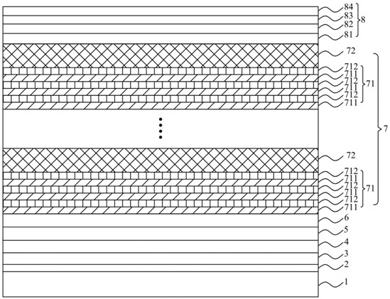
[0038] see figure 1 , is a schematic structural view of a light-emitting diode epitaxial wafer provided by an embodiment of the present invention. For convenience of description, only the parts related to the embodiment of the present invention are shown. The light-emitting diode epitaxial wafer provided by the embodiment of the present invention includes a substrate 1, And a buffer layer 2, a three-dimensional nucleation layer 3, a two-dimensional recovery layer 4, an undoped GaN layer 5, an N-type GaN layer 6, a multi-quantum well layer 7 and a P-type layer 8 sequentially stacked on the substrate 1; Wherein the multi-quantum well layer 7 includes x periodically alternately arranged mixed-polarity quantum well layers 71 and quantum barrier layers 72; the mixed-polarity quantum well layer 71 includes y periodically alternately arranged N-polar surface quantum wells Layer 711 and Ga polar surface quantum well layer 712.

[0039] Wherein, in one embodiment of the present invent...

Embodiment 2

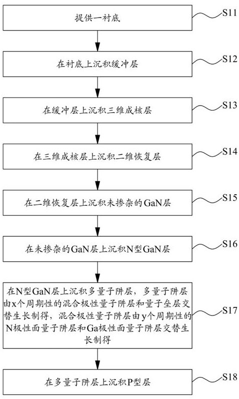
[0050] see figure 2 , shows the method for preparing a light-emitting diode epitaxial wafer in the second embodiment of the present invention, and the method specifically includes steps S11 to S18.

[0051] Step S11, providing a substrate.

[0052] Among them, in the embodiment of the present invention, the selected substrate can be any one of a sapphire substrate, a silicon substrate, a silicon carbide substrate, and a gallium nitride substrate. Specifically, in this embodiment, sapphire is used as the Epitaxial layer growth substrate.

[0053] Further, the present invention adopts metal organic chemical vapor deposition (MOCVD) equipment to grow epitaxial wafers. Among them, high-purity ammonia gas (NH 3 ) as N (nitrogen) source, trimethylgallium (TMGa) and triethylgallium (TEGa) as Ga (gallium) source, trimethylindium (TMIn) as In (indium) source, trimethylaluminum (TMAl ) as the Al (aluminum) source, where silane (SiH 4 ) as an N-type dopant, magnesiumocene (CP 2 Mg...


PUM

PropertyMeasurementUnit
thicknessaaaaaaaaaa
thicknessaaaaaaaaaa
thicknessaaaaaaaaaa

Abstract

The invention provides a light-emitting diode epitaxial wafer and a preparation method thereof. The light-emitting diode epitaxial wafer comprises a substrate, and a buffer layer, a three-dimensional nucleating layer, a two-dimensional recovery layer, an undoped GaN layer, an N-type GaN layer, a multi-quantum well layer and a P-type layer which are sequentially stacked on the substrate, the multi-quantum well layer comprises x mixed polarity quantum well layers and quantum barrier layers which are periodically and alternately arranged; and the mixed polarity quantum well layer comprises y N polar surface quantum well layers and Ga polar surface quantum well layers which are periodically and alternately arranged. The quantum well solves the problem that the luminous efficiency of an LED epitaxial wafer is reduced due to energy band bending and inclination caused by a polarization electric field in an existing quantum well.

Description

technical field [0001] The invention relates to the field of photoelectric technology, in particular to a light-emitting diode epitaxial wafer and a preparation method thereof. Background technique [0002] GaN-based light-emitting diodes (LEDs) are widely used in daily lighting, mobile phone backlights, automotive lights and other fields. The preparation of LED epitaxial wafers is an important part of the preparation of light-emitting diodes. Currently, GaN epitaxial layers grown by metal-organic chemical vapor deposition (MOCVD) are used to prepare LED epitaxial wafers, mainly Ga-Polar GaN thin films. [0003] GaN crystal structure Because the electronegativity of N atoms is stronger than that of Ga atoms, in GaN crystals, the bonding electrons of the covalent bonds between Ga atoms and N atoms will shift, and the electrons will shift to be close to N atoms and away from Ga atoms. , resulting in a polarized electric field in the GaN crystal. There are piezoelectric polari...

Claims


Application Information

Patent Timeline
Patent Type & Authority Applications(China)
IPC IPC(8): H01L33/06H01L33/18H01L33/32H01L33/00
CPCH01L33/06H01L33/18H01L33/32H01L33/007
Inventor 侯合林谢志文张铭信陈铭胜
Owner JIANGXI ZHAO CHI SEMICON CO LTD
Why Eureka
Try Eureka