Solar cell and preparation method thereof

A technology of solar cells and silicon cells, applied in the field of solar cells, can solve the problems of deteriorating the long-term stability of perovskite cells, affecting the performance of perovskite devices, and mismatching components of perovskite layers, so as to inhibit ion migration, Effect of reducing light reflection loss and dense deposition

Pending Publication Date: 2022-05-06
LONGI SOLAR TECH (XIAN) CO LTD
View PDF0 Cites 0 Cited by
  • Summary
  • Abstract
  • Description
  • Claims
  • Application Information

AI Technical Summary

Problems solved by technology

The halide ions (I, Br, Cl) and metal ions (Pb, Sn, etc.) of the perovskite layer in the perovskite battery will cause ion migration due to the defects of the perovskite film layer, and these migrating ions will pass through the hole The transport layer / perovskite layer interface and the perovskite layer / electron transport layer interface cause perovskite layer component mismatch and electrode corrosion, which ultimately deteriorates the long-term working stability of the perovskite cell
In addition, defects in the perovskite film layer can also cause serious performance hysteresis of the device, which seriously affects the performance of the perovskite device.

Method used


Image

  • Solar cell and preparation method thereof
  • Solar cell and preparation method thereof
  • Solar cell and preparation method thereof

Examples


preparation example Construction

[0081] The method for preparing the first stacked perovskite battery includes the following steps:

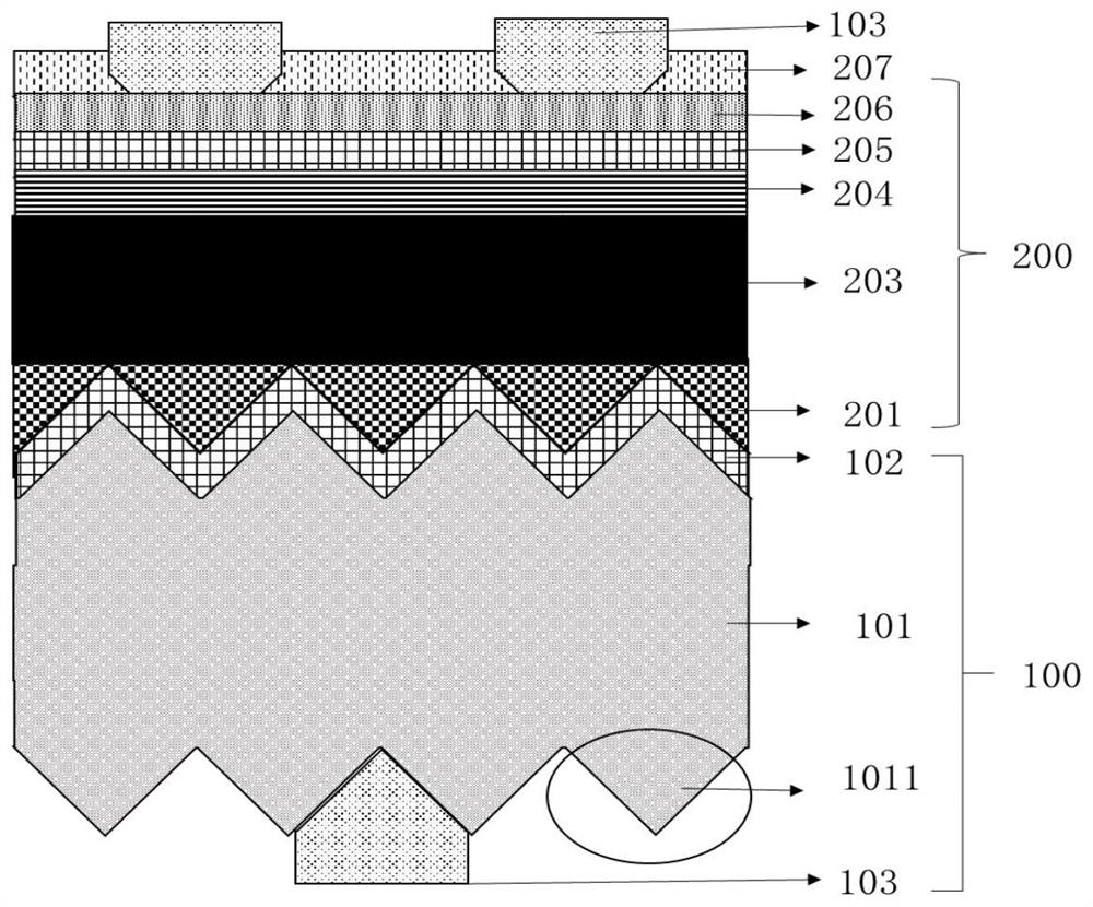
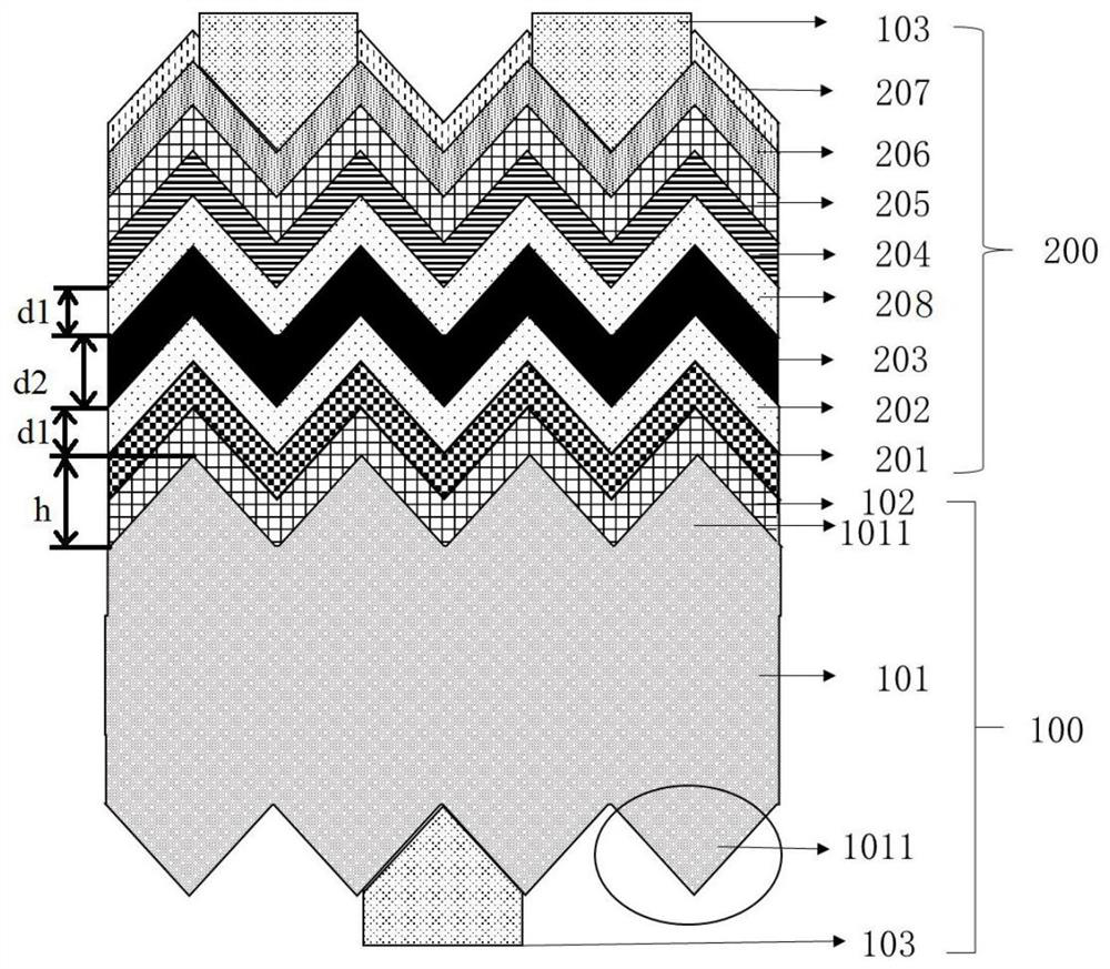
[0082] Step 1: providing the lower battery 100 with the suede structure 1011;

[0083] Step 2: forming a first carrier transport layer 201 on the surface of the lower battery 100;

[0084] Step 3: forming a first interface passivation layer 202 conformal to the textured structure 1011 on the surface of the first carrier transport layer 201 away from the lower battery 100 by vapor deposition;

[0085] Step 4: forming a perovskite absorption layer 203 on the surface of the first interface passivation layer 202 away from the first carrier transport layer 201;

[0086] Step 5: forming a second carrier transport layer 204 on the surface of the perovskite absorption layer 203 on the side away from the first interface passivation layer 202 .

[0087] In step 1, the silicon wafer is sequentially subjected to polishing, texturing, coating, cleaning and tunnel junction procedures to form...

Embodiment 1

[0239] This embodiment is the first type of stacked perovskite battery, and the preparation method includes the following steps:

[0240] Step 1: providing the lower battery 100 with the suede structure 1011;

[0241] Specifically, an n-type silicon wafer of 180 μm and a resistivity of 5Ω.cm commercial grade M2 ​​was polished, textured, and cleaned to form a silicon wafer substrate with a textured structure 1011 through alkaline solution polishing, and PECVD was used on the light incident side of the cell. (Plasma Enhanced Chemical Vapor Deposition, plasma enhanced chemical vapor deposition method) process to prepare the tunneling layer 102, the tunneling layer 102 can use PECVD to deposit uc-Si-p respectively + Layers and uc-Si-n + The layer forms a tunnel junction with a thickness of 30 nm.

[0242] Step 2: forming a first carrier transport layer 201 on the surface of the lower battery 100;

[0243] Specifically, by vacuum evaporation (the rate of evaporation is ) On th...

Embodiment 2

[0256] This embodiment is a second type of stacked perovskite battery, and the preparation method includes the following steps:

[0257] Step 1: providing the lower battery 100 with the suede structure 1011;

[0258] Specifically, an n-type silicon wafer of 180 μm and a resistivity of 5Ω.cm commercial grade M2 ​​was polished, textured, and cleaned to form a silicon wafer substrate with a textured structure 1011 through alkaline solution polishing, and PECVD was used on the light incident side of the cell. (Plasma Enhanced Chemical Vapor Deposition, Plasma Enhanced Chemical Vapor Deposition) process to prepare the tunneling layer 102, the tunneling layer 102 can use PECVD to deposit uc-Si-p respectively + Layers and uc-Si-n + The layer forms a tunnel junction with a thickness of 30 nm.

[0259] Step 2: forming a first carrier transport layer 201 on the surface of the lower battery 100;

[0260] Specifically, by vacuum evaporation (the rate of evaporation is ) On the tunnel...


PUM

PropertyMeasurementUnit
Heightaaaaaaaaaa
Thicknessaaaaaaaaaa
Thicknessaaaaaaaaaa

Abstract

The invention discloses a solar cell which comprises a substrate, the surface of the substrate is provided with a suede structure, and the substrate is provided with a carrier transport layer and a perovskite absorption layer which are arranged in a stacked mode. An interface passivation layer is arranged between the perovskite absorption layer and the carrier transmission layer, and the interface passivation layer and the suede structure are conformal. The invention also provides a preparation method of the solar cell. According to the solar cell provided by the invention, the interface passivation layer and the textured surface of the substrate are conformal, so that uniform and compact deposition of the interface passivation layer and the textured surface of the substrate is realized, ion migration is inhibited, and hysteresis of a positive scanning curve and a negative scanning curve of the cell is remarkably reduced; and meanwhile, the conformal structure of the interface passivation layer continues the good light trapping structure design of the substrate textured surface, the light reflection loss is reduced to the maximum extent, and the photo-generated current is remarkably improved.

Description

technical field [0001] The present application relates to the technical field of solar cells, in particular to a solar cell and a preparation method thereof. Background technique [0002] The perovskite cell / silicon-based heterojunction two-end tandem cell realizes spectral distribution absorption, and can obtain a photoelectric conversion efficiency of more than 30% (>29.4% of the silicon cell limit efficiency), which is considered to be the mainstream of low-cost and high-efficiency solar cells in the future. product. To achieve long-term stable operation of perovskite / silicon tandem battery devices, the long-term stability of perovskite cells is crucial. The halide ions (I, Br, Cl) and metal ions (Pb, Sn, etc.) of the perovskite layer in the perovskite cell will cause ion migration due to the defects of the perovskite film, and these migrated ions will pass through the holes. The transport layer / perovskite layer interface and the perovskite layer / electron transport l...

Claims


Application Information

Patent Timeline
IPC IPC(8): H01L31/0236H01L31/0216H01L31/0224H01L31/0687H01L51/42H01L51/44H01L31/18
CPCH01L31/02363H01L31/02168H01L31/022425H01L31/0687H01L31/18H10K30/00H10K30/88Y02E10/544Y02E10/549
Inventor 李勃超何博何永才顾小兵王永磊董鑫丁蕾张富李巧艳
Owner LONGI SOLAR TECH (XIAN) CO LTD
Why Eureka
Try Eureka