Preparation method of multilayer ceramic circuit board

A technology of multi-layer ceramics and circuit boards, applied in multi-layer circuit manufacturing, printed circuit manufacturing, circuits, etc., can solve the problems of low wiring accuracy, wiring accuracy, insufficient yield, low yield, etc., to reduce shrinkage differences, The effect of high yield and easy processing

Pending Publication Date: 2022-05-13
武汉利之达科技股份有限公司 +1
View PDF0 Cites 1 Cited by
  • Summary
  • Abstract
  • Description
  • Claims
  • Application Information

AI Technical Summary

Problems solved by technology

[0005] In order to overcome the shortcomings of existing multilayer ceramic circuit boards in terms of wiring accuracy and yield, and to meet the application requirements in the fields of communications, automobiles, and aerospace, the present invention proposes a method for manufacturing multilayer ceramic circuit boards, which solves the problem of traditional substrates. It can withstand 100-200°C for a long time and realizes the miniaturization and high integration density of multilayer ceramic substrates.

Method used


Image

  • Preparation method of multilayer ceramic circuit board
  • Preparation method of multilayer ceramic circuit board
  • Preparation method of multilayer ceramic circuit board

Examples


Embodiment 1

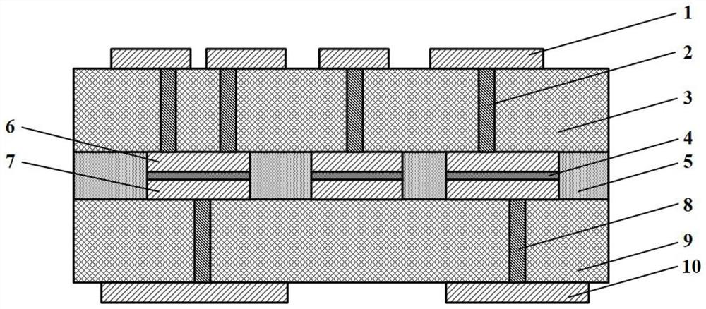
[0038] In this embodiment, the metal solder is SnAgCu solder paste.

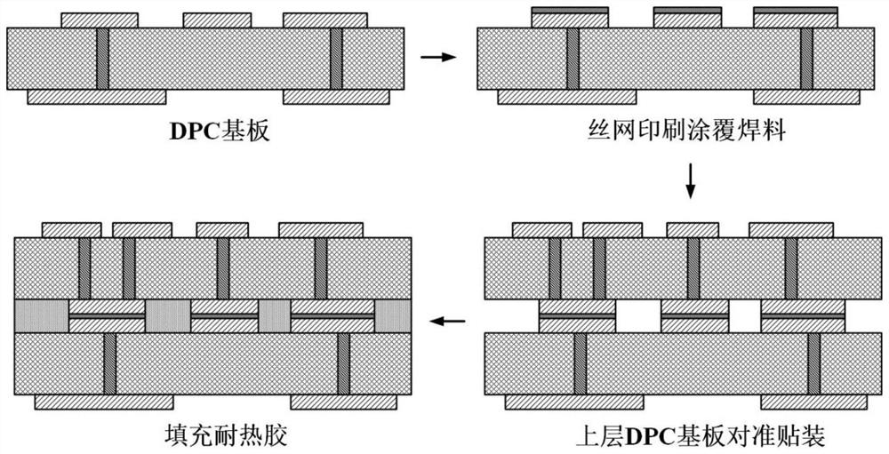
[0039] In this embodiment, realizing the bonding between the DPC ceramic substrate 3 and the DPC ceramic substrate 9 includes the following steps:

[0040] 1) Degreasing, decontaminating and drying the ceramic substrate 3 and the ceramic substrate 9 and their metal layers;

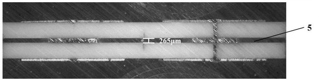
[0041] 2) Coating the SnAgCu solder paste onto the metal layer 7 of the ceramic substrate 9 by screen printing, with a thickness of 40 μm;

[0042] 3) Align the ceramic substrate 3 with the metal layer on the ceramic substrate 9, adopt a solder bonding process, and make SnAgCu under the process conditions of a maximum bonding temperature of 280 ° C, a bonding pressure of 2 MPa, and a bonding time of 15 minutes. The solder is bonded to the substrate, thereby realizing the mechanical connection and electrical interconnection of the two ceramic substrates.

Embodiment 2

[0044] In this embodiment, AuSn solder is selected as the metal solder.

[0045] In this embodiment, realizing the bonding between the DPC ceramic substrate 3 and the DPC ceramic substrate 9 includes the following steps:

[0046] 1) Degreasing, decontaminating and drying the ceramic substrate 3 and the ceramic substrate 9 and their metal layers;

[0047] 2) AuSn solder is deposited on the metal layer 7 of the ceramic substrate 9 by a physical vapor deposition (CVD) process, with a thickness of 3 μm;

[0048] 3) Align the ceramic substrate 3 with the metal layer on the ceramic substrate 9, and use the eutectic bonding process under the conditions of the highest bonding temperature of 320° C., the bonding pressure of 10 MPa, and the bonding time of 15 minutes. The AuSn solder is bonded to the substrate, thereby realizing the mechanical connection and electrical interconnection of the two-layer ceramic substrate.

[0049] In the invention of the multi-layer ceramic circuit boar...

Embodiment 3

[0052] In this embodiment, PI polyimide is selected as the high temperature resistant insulating glue. PI glue is a yellow transparent liquid at room temperature, with a viscosity of 30-35Pa s and a thermal expansion coefficient of 3.6×10 -5 / °C.

[0053] In this embodiment, after the ceramic substrate 3 and the ceramic substrate 9 are bonded using SnAgCu solder, the process of filling the heat-resistant glue between the substrates 3 and 9 includes the following steps:

[0054] 1) Use a syringe to pick up the heat-resistant glue and fill it along the edge of the gap between the ceramic substrate layers. The filling method of the syringe is unilateral and unidirectional "I" extrusion;

[0055] 2) Due to the high viscosity of PI glue, lay the substrate flat, use a vacuum pump to pump air at the other end, and fill the entire interlayer with heat-resistant glue through vacuum adsorption;

[0056] 3) According to the processing process, the temperature is raised to 80°C, 120°C, ...


PUM

PropertyMeasurementUnit
thicknessaaaaaaaaaa
thicknessaaaaaaaaaa
thicknessaaaaaaaaaa

Abstract

The invention discloses a preparation method of a multilayer ceramic circuit board. The multilayer ceramic circuit board is formed by stacking and bonding a plurality of electroplated ceramic substrates (DPC). The method comprises the following steps: firstly, preparing a DPC ceramic substrate containing a surface circuit layer and vertical interconnection metal columns through a pattern electroplating process; then preparing a metal solder on the circuit layer of the DPC ceramic substrate, stacking and aligning a plurality of DPC ceramic substrates, and then bonding to realize mechanical stable connection and electric interconnection between the DPC ceramic substrates; and finally, filling high-temperature-resistant insulating glue between the DPC substrates, and curing to obtain the multi-layer ceramic circuit board. By utilizing the characteristics of good heat conduction/heat resistance, high pattern precision, vertical interconnection and the like of the DPC ceramic substrates, mechanical connection and electric interconnection between the DPC substrates are realized through metal bonding, the multilayer ceramic circuit board with high reliability and high precision is prepared, and the requirements of miniaturization and integrated packaging of power devices are met.

Description

technical field [0001] The invention belongs to the technical field of microelectronic packaging, and more specifically relates to a method for preparing a multilayer ceramic circuit board, which effectively improves the integration degree of power devices. Background technique [0002] With the continuous development of electronic information technology, the application and update of electronic products are also expanding rapidly, and their functions are also increasing. The third-generation semiconductor materials represented by SiC and GaN have important applications in the fields of automobiles, communications, aerospace, and weapons and equipment due to their large band gap and high breakdown voltage. With the gradual increase in application requirements, chip packaging is also gradually developing towards high reliability, high integration density, and miniaturization. Nowadays, the packaging of chips on a planar substrate is limited by the size of the substrate itsel...

Claims


Application Information

Patent Timeline
Patent Type & Authority Applications(China)
IPC IPC(8): H05K3/46H05K3/18H05K3/42H01L21/48H01L23/498
CPCH05K3/4611H05K3/4623H05K3/423H05K3/18H05K3/4614H05K3/4626H01L21/4857H01L23/49822H01L23/49838H01L23/49894H05K2203/061
Inventor 刘松坡张树强黄卫军
Owner 武汉利之达科技股份有限公司
Why Eureka
Try Eureka