Perovskite light absorption layer, preparation method of perovskite light absorption layer, solar cell and preparation method of solar cell

A solar cell and light-absorbing layer technology, applied in photovoltaic power generation, circuits, electrical components, etc., can solve the problems of poor thermal stability of organic small molecules, affecting perovskite grain structure, poor universality and repeatability, etc., to achieve Improvement of photoelectric conversion efficiency, reduction of carrier non-radiative recombination loss, and improvement of crystallization performance

Pending Publication Date: 2022-05-27
SOUTH CHINA UNIV OF TECH
View PDF0 Cites 0 Cited by
  • Summary
  • Abstract
  • Description
  • Claims
  • Application Information

AI Technical Summary

Problems solved by technology

At present, organic small molecules are often added to the perovskite precursor solution to modify and passivate the perovskite film, which can reduce the defects inside and on the surface of the film, but excessive small organic molecules will also reduce the crystallization of the film. properties, and even affect the grain structure of perovskite
In addition, the method of organic small molecule modification is not universal and reproducible. The optimal concentration of organic small molecules varies greatly in different components of perovskite precursor solutions, and the thermal stability of organic small molecules Poor stability, these factors will limit the application of this method in the preparation of all-inorganic perovskite thin films

Method used


Image

  • Perovskite light absorption layer, preparation method of perovskite light absorption layer, solar cell and preparation method of solar cell
  • Perovskite light absorption layer, preparation method of perovskite light absorption layer, solar cell and preparation method of solar cell
  • Perovskite light absorption layer, preparation method of perovskite light absorption layer, solar cell and preparation method of solar cell

Examples


Embodiment

[0048] A kind of solar cell, its preparation method comprises the following steps:

[0049] 1) The glass substrate coated with the ITO layer (that is, the cathode layer) is cleaned by ultrasonic cleaning with acetone, semiconductor detergent, deionized water and isopropanol successively, and then placed in a constant temperature oven for drying for subsequent use;

[0050] 2) Place the glass substrate treated in step 1) in a vacuum plasma cleaner for 3 min, and then dilute the ZnO nanoparticle ink with a mass fraction of 2.5% with isopropyl alcohol (IPA) at a volume ratio of 1:7 and spin it. Coated on the surface of the ITO layer of the glass substrate, the spin coating speed is 3000rpm, the time is 30s, and then the mass fraction of 15% SnO 2 The colloidal dispersion was diluted with deionized water at a volume of 1:6.5 and then spin-coated for the second time. The spin-coating speed was 3000 rpm for 30 s, and then annealed at 150 °C for 30 min in the atmospheric environment ...


PUM

PropertyMeasurementUnit
Thicknessaaaaaaaaaa
Thicknessaaaaaaaaaa
Thicknessaaaaaaaaaa

Abstract

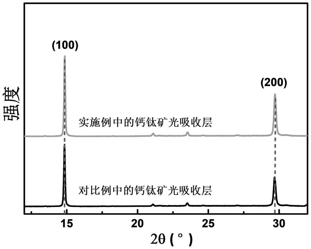
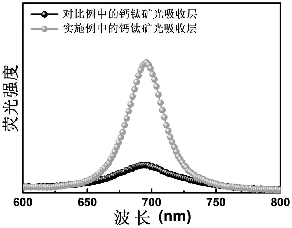
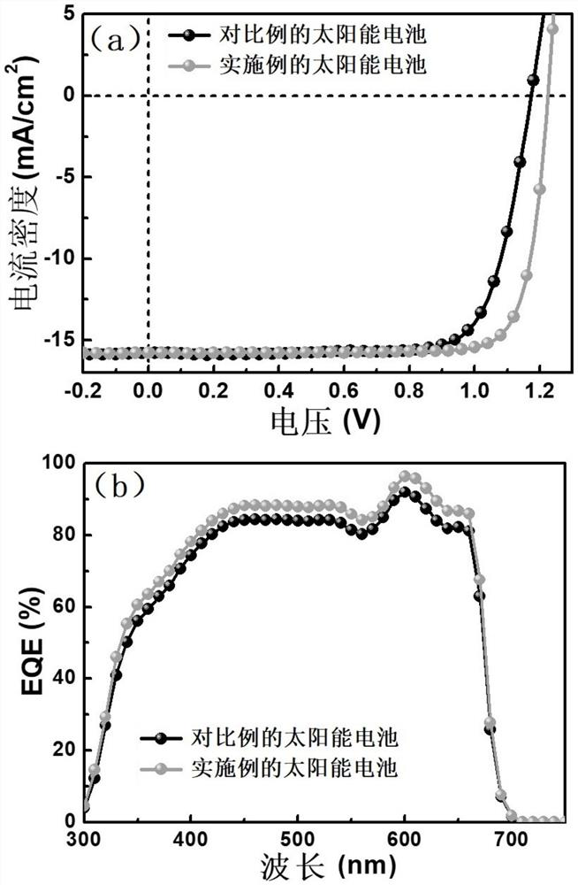
The invention discloses a perovskite light absorption layer and a preparation method thereof, and a solar cell and a preparation method thereof. The preparation method of the perovskite light absorption layer comprises the following steps: 1) depositing a perovskite thin film on a substrate; 2) heating the perovskite thin film at 45-50 DEG C for 60-70 seconds, annealing the perovskite thin film at 280-320 DEG C for 60-70 seconds, and naturally cooling the perovskite thin film; and 3) annealing the perovskite thin film treated in the step 2) at the temperature of 60-120 DEG C for 10-20 minutes. According to the invention, secondary annealing treatment is carried out on the perovskite light absorption layer after high-temperature annealing and cooling, so that recrystallization of the polycrystalline perovskite thin film is promoted through Ostwald curing, the grain size of the perovskite thin film is increased, the crystallization performance of the perovskite thin film is improved, and the yield of the perovskite thin film is improved. The carrier non-radiative recombination loss of the solar cell containing the perovskite light absorption layer is significantly reduced, and the photoelectric conversion efficiency is significantly improved.

Description

technical field [0001] The invention relates to the technical field of solar cell devices, in particular to a perovskite light absorption layer and a preparation method thereof, a solar cell and a preparation method thereof. Background technique [0002] Perovskite materials have the advantages of large absorption coefficient, high carrier mobility, long electron-hole diffusion distance, and easy adjustment of the band gap. Moreover, there are abundant reserves of perovskite raw materials on the earth, low cost, and easy mass production. , has good commercial potential, therefore, perovskite solar cells have become a research hotspot in the field of photovoltaics. [0003] All-inorganic perovskite (CsPbX 3 , X is I or Br) does not contain organic components, has excellent thermal stability and high charge mobility, and has a wide band gap (1.7eV ~ 2.3eV), is an ideal front electrode material for tandem batteries . [0004] The intrinsic film quality of the perovskite ligh...

Claims


Application Information

Patent Timeline
IPC IPC(8): H01L31/18H01L31/0725
CPCH01L31/1864H01L31/1872H01L31/0725Y02E10/50
Inventor 薛启帆周颖芝周志升
Owner SOUTH CHINA UNIV OF TECH
Why Eureka
Try Eureka