Nitride epitaxial layer preparation method and semiconductor epitaxial wafer thereof

A nitride epitaxial layer and nitride semiconductor technology, which is applied in semiconductor devices, chemical instruments and methods, and chemically reactive gases, etc., can solve the problems of high dislocation density of crystal materials, restricting applications, and potential safety hazards. The effect of improving uniformity and nucleation density, facilitating large-scale production and reducing the risk of contamination

Active Publication Date: 2022-06-03
JIANGSU INST OF ADVANCED SEMICON CO LTD
View PDF6 Cites 2 Cited by
  • Summary
  • Abstract
  • Description
  • Claims
  • Application Information

AI Technical Summary

Problems solved by technology

[0003] At present, the more mature MOCVD epitaxy technology for preparing GaN materials is the epitaxy technology grown on heterogeneous substrates. Due to the lattice and thermal expansion mismatch between the substrate and the epitaxial layer, the dislocation density and stress of the epitaxially grown crystal material are high. Larger, prone to warping cracks and other phenomena, affecting the working efficiency and life of the device, restricting its application in the field of semiconductor electronics
[0004] In MOCVD epitaxy technology, the MO source precursor material is the key material and dopant for epitaxial growth of semiconductor compounds. To obtain high-quality epitaxial layers, doping and defects must be strictly controlled. Generally speaking, the higher the purity of the MO source, the lower the impurities. Less, the higher the quality of the product, try to avoid the introduction of impurities in the epitaxial growth process, in the MOCVD epitaxial growth process O as an impurity source of unintentional doping, will introduce deep level defects in the nitride epitaxial layer, nitride The yellow band luminescence in the epitaxial layer is one of the judgments of poor growth quality of the nitride epitaxial layer. It is generally considered to be a deep level defect related to O. The introduction of O impurities in the epitaxial growth must be strictly controlled. Currently, MO source precursor materials During the synthesis process, in order to obtain high-purity MO precursors, the MO source precursor materials must be purified to remove impurities such as O. However, the purification process has high requirements for equipment airtightness, poor safety, and potential safety hazards. Increase the MO source Preparation cost, so the most fundamental thing to evaluate the quality of MO source precursor material is to see whether the photoelectric performance of the product obtained by using the MO source epitaxy is good or bad, whether it meets the device performance requirements and the cost level

Method used


Image

  • Nitride epitaxial layer preparation method and semiconductor epitaxial wafer thereof
  • Nitride epitaxial layer preparation method and semiconductor epitaxial wafer thereof
  • Nitride epitaxial layer preparation method and semiconductor epitaxial wafer thereof

Examples


preparation example Construction

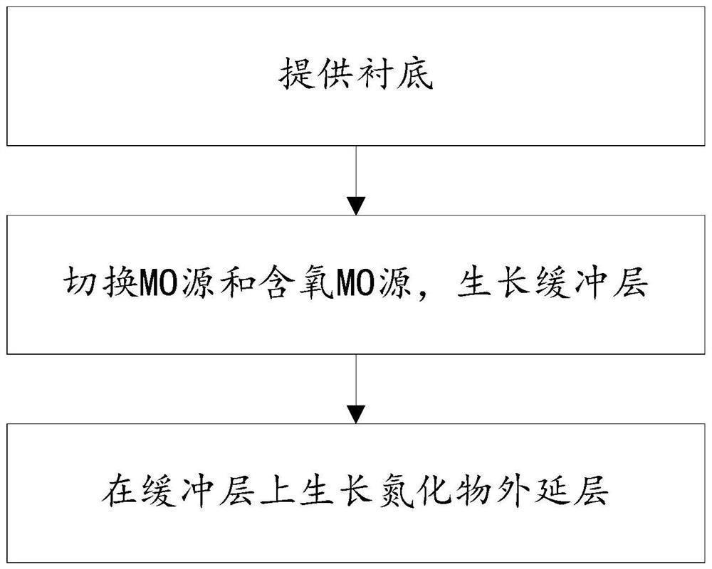
[0037] like figure 1 As shown, the present invention provides a method for preparing a nitride epitaxial layer, comprising the following steps:

[0038] S1: Provide substrate;

[0039] S2: growing a buffer layer on the substrate, wherein the buffer layer includes a nitride buffer layer and an oxygen-containing buffer layer grown by alternately switching the MO source and the oxygen-containing MO source as precursor materials through periodic cycles;

[0040] S3: A nitride epitaxial layer is grown on the buffer layer.

[0041] Specifically, in the MOCVD reaction chamber, the preparation method includes the following steps:

[0042] 1) Provide a substrate, under the conditions of temperature 900 ~ 1200 ℃, growth pressure 50 ~ 650torr, H 2 Atmospheric heat treatment for 1 to 10 minutes;

[0043] 2) On the substrate, under the conditions of a temperature of 500-1000° C. and a growth pressure of 50-650 torr, a buffer layer of 10-100 nm is grown, wherein: the growth of the buffe...

Embodiment 1

[0065] In this example, the alternate growth of GaON and GaN buffer layers with oxygen-containing TMG sources and TMG sources, and the preparation of gallium nitride epitaxial layers in Comparative Example 1 and Comparative Example 2 are used to illustrate the effect. All the preparation environments are placed in the MOCVD reaction chamber. Inside.

[0066] In this embodiment, the gallium nitride epitaxial layer is prepared by alternately growing GaON and GaN buffer layers with an oxygen-containing TMG source and a TMG source, including the following steps:

[0067] 1) Provide sapphire substrate, H 2 Atmospheric heat treatment for 5min;

[0068] 2) On the sapphire substrate, at a temperature of 540 °C and a growth pressure of 300 torr, periodically and alternately grow a GaON buffer layer with a thickness of 3 nm and a GaN buffer layer with a thickness of 5 nm for 20 cycles. The source is oxygen-containing TMG source, the growth GaN buffer layer is switched to TMG source, a...

Embodiment 2

[0081]In this example, a gallium nitride epitaxial layer is prepared by alternately growing a buffer layer of GaON and GaN and a pure TMG source with an oxygen content of less than 1 ppm by alternately growing a TMG source containing oxygen and a TMG source to illustrate the effect, which is different from the first example. The difference is that the growth temperature for preparing the gallium nitride epitaxial layer is different, and all the preparation environments are placed in the MOCVD reaction chamber.

[0082] In this embodiment, the gallium nitride epitaxial layer is prepared by alternately growing GaON and GaN buffer layers with an oxygen-containing TMG source and a TMG source, including the following steps:

[0083] 1) Provide sapphire substrate, H 2 Atmospheric heat treatment for 5min;

[0084] 2) On a sapphire substrate, under the conditions of a temperature of 540 °C and a growth pressure of 300 torr, a GaON buffer layer with a thickness of 3 nm and a GaN buffe...


PUM

PropertyMeasurementUnit
thicknessaaaaaaaaaa
thicknessaaaaaaaaaa
thicknessaaaaaaaaaa

Abstract

The invention discloses a nitride epitaxial layer preparation method and a semiconductor epitaxial wafer thereof. The method comprises the following steps: providing a substrate; a buffer layer is grown on the substrate, the buffer layer comprises a nitride buffer layer and an oxygen-containing buffer layer, and the nitride buffer layer and the oxygen-containing buffer layer are grown by alternately switching an MO source and an oxygen-containing MO source in a periodic cycle mode to serve as precursor materials; and growing a nitride epitaxial layer on the buffer layer. The oxygen-containing buffer layer is grown through the oxygen-containing MO source process, on one hand, the in-situ growth oxygen-containing buffer layer has good lattice mismatch relaxation, relieves lattice adaptation and releases the stress of the substrate and the epitaxial layer, and a high-quality gallium nitride epitaxial layer with low dislocation density can be obtained; the distribution uniformity and nucleation density of oxygen-containing buffer crystal grains are improved, and a high-quality nitride epitaxial layer is obtained; on the other hand, the technological process is simple, pollution risks in the substrate and epitaxial layer transfer process are reduced, repeatability is good, and large-scale production is facilitated.

Description

technical field [0001] The invention relates to the technical field of semiconductors, in particular to a method for preparing a nitride epitaxial layer and a semiconductor epitaxial wafer thereof. Background technique [0002] The wide-bandgap semiconductor material GaN has excellent physical and chemical properties such as high breakdown field strength, high thermal conductivity, and fast electron saturation migration rate. attention has been paid to its application prospects. [0003] At present, the more mature MOCVD epitaxy technology for preparing GaN materials is an epitaxy technology grown on a heterogeneous substrate. Due to the mismatch between the lattice and thermal expansion between the substrate and the epitaxial layer, the dislocation density and stress of the epitaxially grown crystal material are high. Larger, warping cracks and other phenomena are prone to occur, which affects the working efficiency and life of the device, and restricts its application in ...

Claims


Application Information

Patent Timeline
Patent Type & Authority Applications(China)
IPC IPC(8): C30B25/18C30B25/14C30B29/40H01L33/00H01L33/06H01L33/12
CPCC30B25/183C30B25/14C30B29/406H01L33/007H01L33/12H01L33/06Y02P70/50
Inventor 闫其昂王国斌
Owner JIANGSU INST OF ADVANCED SEMICON CO LTD
Why Eureka
Try Eureka