Self-driven solar blind photoelectric detector based on p-type indium acid cuprous single crystal thin film and preparation method of self-driven solar blind photoelectric detector

A technology of photodetectors and single crystal thin films, applied in circuits, electrical components, semiconductor devices, etc., can solve problems such as difficult to cover sun-blind bands, large lattice mismatch rates, etc., achieve excellent detection performance and reduce defect density , arrange the complete effect

Pending Publication Date: 2022-07-22
SHANDONG UNIV
View PDF5 Cites 0 Cited by
  • Summary
  • Abstract
  • Description
  • Claims
  • Application Information

AI Technical Summary

Problems solved by technology

However, this material is not only compatible with GaN, ZnO and SnO 2 Equal wide bandgap semiconductor materials have a large lattice mismatch rate, and their forbidden band width is only 3.5eV, it is difficult to cover the entire solar-blind band, especially the solar-blind light near 200nm

Method used


Image

  • Self-driven solar blind photoelectric detector based on p-type indium acid cuprous single crystal thin film and preparation method of self-driven solar blind photoelectric detector
  • Self-driven solar blind photoelectric detector based on p-type indium acid cuprous single crystal thin film and preparation method of self-driven solar blind photoelectric detector
  • Self-driven solar blind photoelectric detector based on p-type indium acid cuprous single crystal thin film and preparation method of self-driven solar blind photoelectric detector

Examples


Embodiment 1

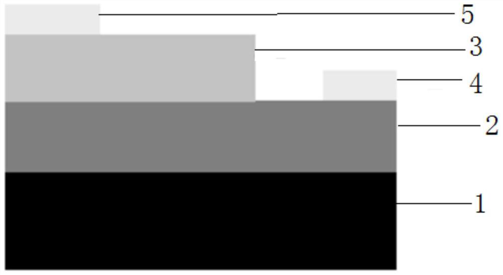
[0040] like figure 1 As shown, a self-driven solar-blind photodetector based on a p-type cuprous indium single crystal thin film, the self-driven solar-blind photodetector includes a substrate 1, and an n-type wide-bandgap semiconductor single-crystal film is arranged above the substrate 1 Crystal thin film 2, a p-type cuprous indium single crystal thin film 3 and a first electrode 4 are arranged above the n-type wide band gap semiconductor single crystal thin film 2, and the p-type cuprous indium single crystal thin film 3 and the first electrode 4 The space is a blank area; a second electrode 5 is arranged above the p-type cuprous indium single crystal thin film 3 .

[0041] The substrate 1 is a sapphire substrate. The n-type wide band gap semiconductor single crystal thin film 2 is Si-doped gallium nitride (GaN, and ). The thickness of the n-type wide band gap semiconductor single crystal thin film 3 is 2 μm, and the carrier concentration is 5×10 18 Pieces / cm 3 .

...

Embodiment 2

[0046] A self-driven solar-blind photodetector based on a p-type cuprous indate single crystal thin film, the structure is as described in Embodiment 1, the difference is that the substrate 1 is a zinc oxide substrate, and the n-type The wide band gap semiconductor single crystal thin film 2 is a hexagonal zinc oxide (ZnO, and ), the p-type cuprous indate single crystal film 3 is a Ca-doped p-type cuprous indate single crystal film, and the doping concentration of Ca is 5%.

Embodiment 3

[0048] The preparation method of the self-driven solar-blind photodetector based on the p-type cuprous indium single crystal thin film described in Embodiment 1 specifically includes the following steps:

[0049] (1) Clean the sapphire substrate covered by the gallium nitride film;

[0050] (2) The Cu 2 O-In 2 O 3 The ceramic target and substrate are respectively placed in the corresponding positions of the target and substrate in the reaction chamber, and the reaction chamber is closed; the side pumping path is opened, the air in the reaction chamber is pumped to a low vacuum state, and the side pumping path is closed; the molecular pump is turned on. , open the chamber gate valve, and pump the reaction chamber to a high vacuum of 8×10 -5 Pa, heated to 750°C;

[0051] (3) open the high-purity oxygen cylinder, feed high-purity oxygen (5N) into the reaction chamber, and the oxygen flow rate is 20sccm, adjust the gate valve of the reaction chamber, and control the pressure o...


PUM

PropertyMeasurementUnit
thicknessaaaaaaaaaa
thicknessaaaaaaaaaa
thicknessaaaaaaaaaa

Abstract

The invention relates to a self-driven solar blind photoelectric detector based on a p-type indium acid cuprous single crystal thin film and a preparation method of the self-driven solar blind photoelectric detector. The self-driven solar blind photoelectric detector comprises a substrate, an n-type wide-band-gap semiconductor single crystal thin film is arranged above the substrate, a p-type cuprous indate single crystal thin film and a first electrode are arranged above the n-type wide-band-gap semiconductor single crystal thin film, and a blank area is formed between the p-type cuprous indate single crystal thin film and the first electrode; and a second electrode is arranged above the p-type indium acid cuprous single crystal thin film. The self-driven solar-blind photoelectric detector prepared by the invention has more excellent detection performance, realizes solar-blind wave band self-driven detection of the device by applying zero bias under the irradiation of a solar-blind light source, has higher photoelectric sensitivity, and can be widely applied to special environments such as space, seabed and the like.

Description

technical field [0001] The invention relates to a self-driven solar-blind photodetector based on a p-type cuprous indium single crystal thin film and a preparation method thereof, belonging to the technical field of semiconductor photoelectric materials and devices. Background technique [0002] The solar-blind photodetector is a type of optoelectronic device that can convert the solar-blind band ultraviolet (200-280nm) signal into an electrical signal. It can play an important role in many key application scenarios such as missile tracking, fire warning and deep space detection. . At present, the commonly used materials for preparing solar-blind UV photodetectors are AlGaN, MgZnO, and Ga. 2 O 3 Equal wide band gap semiconductor material. for Al x Ga 1-x N, Mg x Zn 1-x The O material must be adjusted by the composition of the alloy to adjust the band gap to achieve the purpose of solar blind detection, but the fluctuation of the doping ratio will affect the detection ...

Claims


Application Information

Patent Timeline
Patent Type & Authority Applications(China)
IPC IPC(8): H01L31/036H01L31/032H01L31/0336H01L31/0304H01L31/109H01L31/18
CPCH01L31/0321H01L31/0336H01L31/03042H01L31/03044H01L31/109H01L31/036H01L31/18
Inventor 肖洪地冯博栾彩娜
Owner SHANDONG UNIV
Why Eureka
Try Eureka