
Semiconductor combustible gas sensor based on MEMS technology and preparation method thereof

A gas sensor and semiconductor technology, applied in the direction of air quality improvement, material resistance, etc., can solve the problems of increased energy consumption of gas sensors, difficulty in ensuring product consistency, increased heat loss, etc., to achieve simple and easy preparation process and avoid warping , increase the binding effect

Active Publication Date: 2022-08-02
河南森斯科传感技术有限公司
View PDF12 Cites 0 Cited by
  • Summary
  • Abstract
  • Description
  • Claims
  • Application Information

AI Technical Summary

Problems solved by technology

The patent said that there is no direct heat conduction between the heating unit and the gas-sensitive structure, and the complete contact between the heating layer and the substrate also increases heat loss, resulting in increased energy consumption of the gas sensor; at the same time, the multiple interwoven porous conductive structures of the gas-sensitive structure Fibers are formed from sulfonated graphene and thiophene oligomers treated in a specific environment. There are many influencing parameters, and product consistency is not easy to guarantee.

Method used


Image

  • Semiconductor combustible gas sensor based on MEMS technology and preparation method thereof
  • Semiconductor combustible gas sensor based on MEMS technology and preparation method thereof
  • Semiconductor combustible gas sensor based on MEMS technology and preparation method thereof

Examples


Embodiment 1

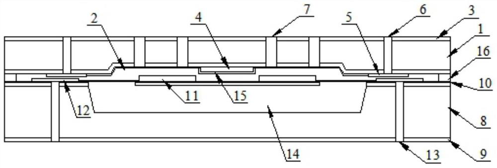
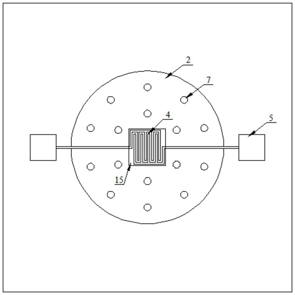
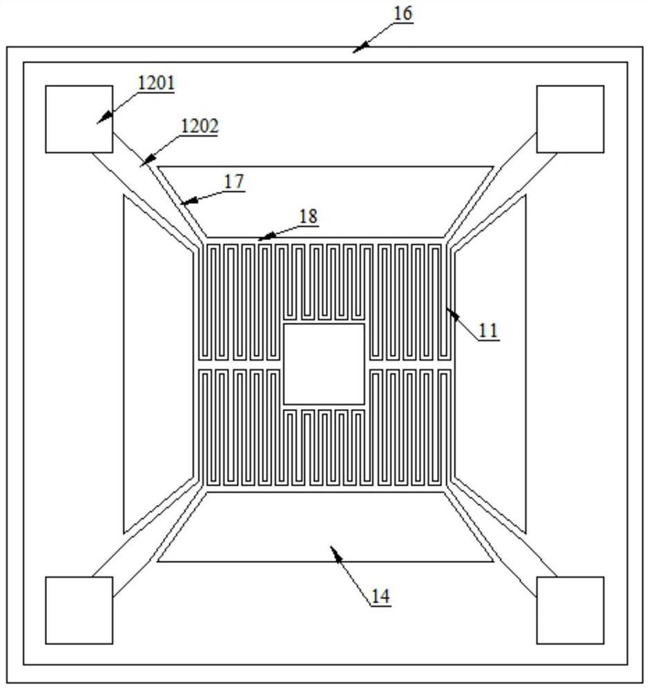
[0022] like Figures 1 to 3 As shown, a semiconductor combustible gas sensor based on MEMS technology includes a gas sensing module and a heating module arranged oppositely, and the gas sensing module and the heating module are bonded and connected. The outer edge of the upper surface of the heating module is provided with a gasket 16, and the gasket 16 is connected between the heating module and the gas sensing module.

[0023] The gas sensor module includes a silicon substrate 1, a groove 2 is provided on the lower side of the silicon substrate 1, and a first insulating layer 3 is formed on the upper and lower sides of the silicon substrate 1, and the first insulating layer on the lower side is formed. 3, a test electrode 4 and a test conductive strip 5 are sputtered on the test electrode 4, and a gas-sensitive coating 15 is coated on the test electrode 4, and the gas-sensitive coating 15 contains semiconductor metal oxides, precious metal catalysts, catalyst carriers and ac...

Embodiment 2

[0041] like Figure 5 As shown, since the test conductive strip 5 does not overlap with the heating electrode 11 and the heating conductive strip 12, the first lead hole 6 can be arranged on the heating module, and the test electrode 4 can pass the test conductive strip 5, the first lead Holes 6 are routed to the bottom surface of the heating module, which helps further facilitate sensor packaging.

[0042] The difference between Example 2 and Example 1 is that the gasket 16 is no longer arranged between the heating module and the gas sensor module, the depth of the groove 2 in the gas sensor module is increased to 40 μm, and the first A lead hole 6 , a first lead hole 6 is provided at the portion of the heating module corresponding to the end of the test conductive strip 5 .

Embodiment 3

[0044] According to the structure of the semiconductor combustible gas sensor described in Embodiment 1, in order to improve the consistency and stability of the gas-sensitive coating 15, the specific coating steps are as follows:

[0045] (a) Prepare the raw materials for the mixed slurry:

[0046] 180-220 parts of tin oxide, 72-88 parts of stannous sulfate, 3.6-4.4 parts of pickled asbestos, 45-55 parts of alumina, 6.7-8.3 parts of precious metal catalyst, 6.3-7.7 parts of tungsten trioxide, 3.0-3.8 parts of magnesium oxide parts, 2.7-3.3 parts of vanadium pentoxide, 1.4-1.8 parts of antimony pentoxide, 250-310 parts of tetraethyl silicate, 330-400 parts of formic acid, 100-125 parts of ethylene glycol, 135 parts of N-methylpyrrolidone ~170 parts, 140-175 parts anhydrous ethanol, 180-220 parts pure water;

[0047] This example adopts the optimal formula, specifically: 2.0g of tin oxide, 0.8g of stannous sulfate, 0.04g of pickled asbestos, 0.5g of alumina, 0.06g of platinum ...


PUM

PropertyMeasurementUnit
thicknessaaaaaaaaaa
thicknessaaaaaaaaaa
depthaaaaaaaaaa

Abstract

The invention discloses a semiconductor combustible gas sensor based on MEMS technology, the semiconductor combustible gas sensor comprises a gas sensitive module and a heating module which are oppositely arranged, the gas sensitive module comprises a silicon substrate, a first insulating layer, a test electrode and a test conductive band, and the test electrode is coated with a gas sensitive coating. The gas-sensitive coating contains a semiconductor metal oxide, a noble metal catalyst, a catalyst carrier and acid-washed asbestos, the heating module comprises a silicon substrate, a second insulating layer, a silicon nitride layer, a heating electrode and a heating conductive band, the upper part of the silicon substrate is etched to form a heat insulation cavity, and the heating electrode surrounds the periphery of the test electrode in a surrounding manner; and the heating electrode is not in direct contact with the test electrode. The device is compact in structure and miniaturized in size, reduces energy consumption, improves structural strength, overcomes device damage and attenuation caused by difference of thermal expansion coefficients of all layers of films during working, is good in performance consistency, high in detection sensitivity, large in mechanical strength and long in service life, and has a good application effect and a good industrialization prospect.

Description

technical field [0001] The invention belongs to the technical field of semiconductor gas sensors, in particular to a semiconductor combustible gas sensor based on MEMS technology and a preparation method thereof. Background technique [0002] The semiconductor gas sensor uses metal oxide as the gas sensing material. Its working principle is based on the change of the resistance value of the oxide when the gas to be measured undergoes oxidation / reduction reaction on the surface of the semiconductor metal oxide at a certain working temperature. At present, the most widely used semiconductor gas sensors are mainly based on ceramic tubes and ceramic substrates. Such gas sensors usually require a long time to warm up, and the large volume power consumption is high, which is not conducive to integration and arraying. [0003] With the development of MEMS technology, semiconductor gas sensors can be fabricated on a tiny chip. Low-power semiconductor gas sensors are micro-hot plate ...

Claims


Application Information

Patent Timeline
Patent Type & Authority Applications(China)
IPC IPC(8): G01N27/12
CPCG01N27/127Y02A50/20
Inventor 时学瑞申林王冉石保敬贾毅博赵静靳小丹沈小红宋雨萍杨裕清
Owner 河南森斯科传感技术有限公司
Learn More