Low-power-consumption high-reliability half-packaged trench gate MOSFET device and preparation method thereof
A trench gate, low power consumption technology, applied in semiconductor/solid-state device manufacturing, semiconductor devices, climate sustainability, etc., can solve the problems of increased device on-resistance and increase in conduction loss, and achieve on-resistance Reduced, reduced conduction loss, improved short-circuit capability
- Summary
- Abstract
- Description
- Claims
- Application Information
AI Technical Summary
Problems solved by technology
Method used
Image

Examples
Embodiment 1
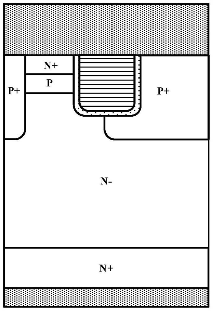
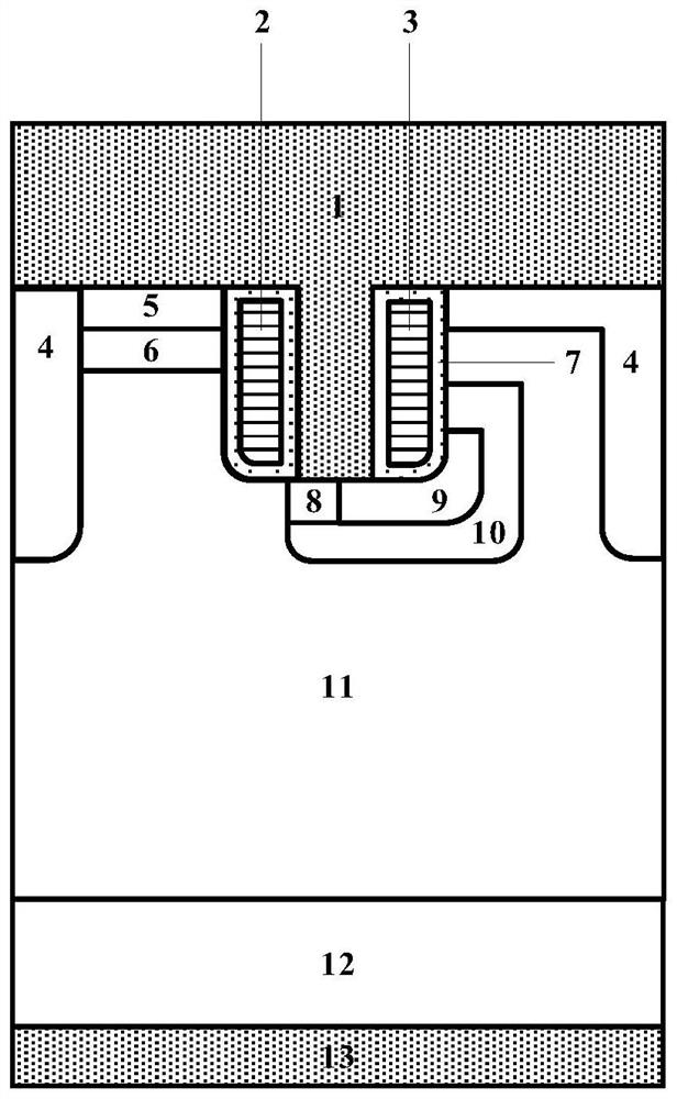
[0051] like figure 2 As shown, a low power consumption semi-encapsulated trench gate silicon carbide MOSFET device in this embodiment includes: an N-type substrate 12 , an N-type epitaxial layer 11 located above the N-type substrate 12 , and an N-type epitaxial layer 11 located above the N-type substrate 12 . The second P-body region 10 above, the second P+ contact region 8 and the second N+ contact region 9 located inside the second P-body region 10, the second P+ contact region 8 and the second N+ contact region 9 located above and The first source electrode 1 forming ohmic contact with the second P+ contact region 8 and the second N+ contact region 9, the gate dielectric 7 on the left and the gate dielectric 7 on the right above the second P-body region 10, the left gate dielectric 7 A trench gate 2 is arranged inside the gate dielectric 7, a sub-trench gate 3 is arranged inside the gate dielectric 7 on the right, and a first P+ contact region 4 located on both sides of th...
Embodiment 2
[0074] like Figure 16 As shown, the difference between the device structure of this embodiment and Embodiment 1 is that there is a second source electrode 14 separated from the first source electrode 1 above the N-type epitaxial layer 11, and the second source electrode 14 is located at the first P+ contact Above the region 4 , the second source electrode 14 forms a Schottky contact with the N-type substrate 11 . The advantage of this is that a Schottky contact is formed between the second source electrode 14 and the N-type epitaxial layer 11, which provides an SBD diode for the MOSFET, which inhibits the opening of the body diode when the MOSFET device works in the third quadrant, so that the device enters bipolar conduction. On mode, the freewheeling capability of the third quadrant of the device is enhanced and the reliability of the device is improved; when the SBD is reverse biased, the JFET formed between the first P+ contact region 4 and the second P-body region 10 is ...
Embodiment 3
[0076] like Figure 18 As shown, a low power consumption trench gate silicon carbide MOSFET device in this embodiment includes: an N-type substrate 12 , an N-type epitaxial layer 11 located above the N-type substrate 12 , and an N-type epitaxial layer 11 located around the top of the N-type epitaxial layer 11 The second P-body region 10 on both sides, the second P+ contact region 8 and the second N+ contact region 9 located inside the second P-body region 10, and above the second P+ contact region 8 and the second N+ contact region 9 The source electrode 1, a gate dielectric 7 is provided in the middle above the N-type epitaxial layer 11, a trench gate 2 is provided inside the gate dielectric 7 in the middle, and a gate dielectric is provided above the second P-body regions 10 on the left and right sides respectively. 7 and the sub-trench gate 3 inside the gate dielectric 7, a first P+ contact region 4 and a first N+ contact region 5 are arranged between the gate dielectric 7 ...
PUM
 Abstract
Description
Claims
Application Information
 - R&D
- Intellectual Property
- Life Sciences
- Materials
- Tech Scout
- Unparalleled Data Quality
- Higher Quality Content
- 60% Fewer Hallucinations
Browse by: Latest US Patents, China's latest patents, Technical Efficacy Thesaurus, Application Domain, Technology Topic, Popular Technical Reports.
© 2025 PatSnap. All rights reserved.Legal|Privacy policy|Modern Slavery Act Transparency Statement|Sitemap|About US| Contact US: help@patsnap.com