Solar cell based on three-dimensional/two-dimensional perovskite and preparation method thereof
A solar cell and perovskite technology, applied in semiconductor/solid-state device manufacturing, circuits, photovoltaic power generation, etc., can solve problems such as poor carrier transmission, and achieve the effects of increased open circuit voltage, good compactness, and improved efficiency
- Summary
- Abstract
- Description
- Claims
- Application Information
AI Technical Summary
Problems solved by technology
Method used
Image
Examples
Embodiment 1
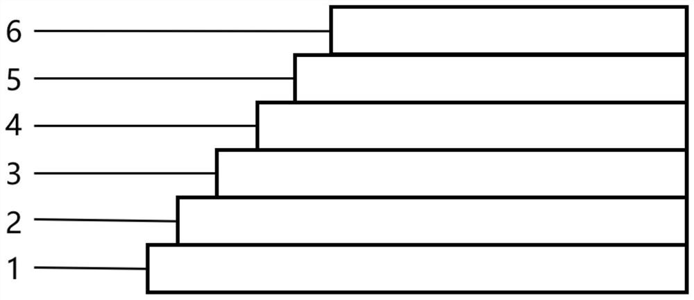
[0042] Based on 3D FAPbI 3 / type two-dimensional (EDBE) PbI 4 The carbon electrode perovskite solar cell with the perovskite active layer, the schematic structure of which is shown in Fig. figure 1 As shown, from bottom to top are the transparent conductive substrate 1, the electron transport layer 2, the three-dimensional perovskite active layer 3, the two-dimensional perovskite active layer 4, the hole transport layer 5 and the counter electrode 6. The specific preparation process as follows:
[0043] Step 1. Clean the FTO substrate:
[0044] The FTO substrate was ultrasonically cleaned with glass cleaning agent, deionized water, and alcohol in sequence for 10 minutes, and then blown dry with a nitrogen gun.
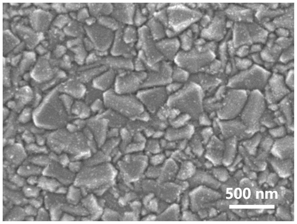
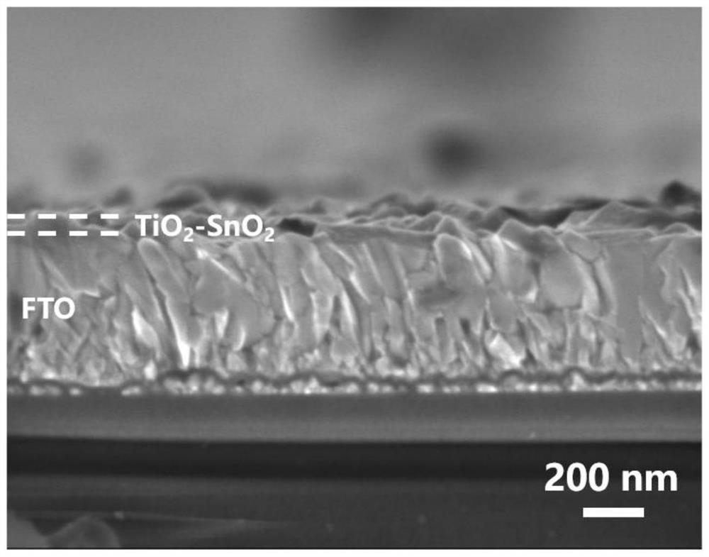
[0045] Step 2. Preparation of electron transport layer TiO 2 -SnO 2 :
[0046] Configure TiO 2 Growth solution: 0.5 mL of titanium tetrachloride (TiCl 4 ) solution was dissolved in a blue bottle containing 100 mL of condensed water, and placed in the refrigera...
Embodiment 2
[0063] 3D MAPbI-based 3 / type two-dimensional (EDBE) PbI 4 Carbon-electrode perovskite solar cells with perovskite active layers
[0064] Other steps are the same as in Example 1, except that:
[0065] The 3D perovskite layer is MAPbI 3 , the concentration is 1.21 mol / L (calculated by the content of lead), specifically including the solute methylamido iodide 1 mmol, lead iodide 1 mmol, and the solvent is successively added as DMF 750 μL, DMSO 72 μL, to obtain 822 μL of precursor solution.
[0066] This embodiment is based on three-dimensional MAPbI 3 / type two-dimensional (EDBE) PbI 4 Perovskite thin films, 3D MAPbI 3 Perovskite thin films and type two-dimensional (EDBE) PbI prepared by the same method 4 X-ray diffraction comparison of perovskite films, such as Figure 8 shown. It can be seen from the figure that the three-dimensional MAPbI 3 / type two-dimensional (EDBE) PbI 4 With (EDBE)PbI at 6.14° 4 The peak of the (020) surface of the 2D perovskite proves that...
Embodiment 3
[0069] 3D MAPbI-based 3 / type two-dimensional (EDBE) PbBr 4 The other steps of the carbon electrode perovskite solar cell with the perovskite active layer are the same as those in Example 1, with the following differences:
[0070] The 3D perovskite layer is MAPbI 3 , the concentration is 1.21 mol / L (calculated by the content of lead), specifically including the solute methylamido iodide 1 mmol, lead iodide 1 mmol, and the solvent is successively added as DMF 750 μL, DMSO 72 μL, to obtain 822 μL of precursor solution.
[0071] Nonlinear long-chain organic amine salt solution is EDBEBr 2 / isopropanol solution at a concentration of 0.66 mg / mL.
[0072] This embodiment is based on three-dimensional MAPbI 3 / type two-dimensional (EDBE) PbBr 4 The comparison of J-V curves of carbon electrode solar cells prepared by perovskite is shown in Fig. Figure 10 It can be seen that the photoelectric conversion efficiency is 16.13%, the open circuit voltage, short circuit current den...
PUM
| Property | Measurement | Unit |
|---|---|---|
| thickness | aaaaa | aaaaa |
| thickness | aaaaa | aaaaa |
| thickness | aaaaa | aaaaa |
Abstract
Description
Claims
Application Information


