Planar electron emitter (PEE), display using it and method for transmitting electron

A technology for electron emission and flat panel display, which is applied in the direction of electrical components, semiconductor devices, and main electrodes of discharge tubes, etc., and can solve problems such as large energy loss, shortened electron mean free path, and large power consumption

Inactive Publication Date: 2005-05-18
彼得・维斯科尔 +3
View PDF19 Cites 2 Cited by
  • Summary
  • Abstract
  • Description
  • Claims
  • Application Information

AI Technical Summary

Problems solved by technology

However, this susceptible electron emitter has other disadvantages: planar electron emitters suitable for this purpose can expose the entire wafer with a wide electron beam, but, at the necessary voltage, due to the necessary high electric field and short distance effect resulting in the extremely short lifetime of these planar electron emitters
[0065] A disadvantage of existing field emission planar electronic devices is that high external voltages must be applied over relatively short distances (on the order of the mean free path of electrons) in order to generate an electric field high enough to facilitate the emission and acceleration of electrons.
[0066] Another disadvantage is that this requirement to apply a relatively high local electric field over a relatively short distance, together with the quality of the material obtained, results in a shortened electron mean free path (increased scattering ratio), which in turn results in establishes a limit on the possible practical distances within the device that electrons can travel without too appreciable loss of energy
[0067] There is also the disadvantage that, due to the results mentioned above, only a fraction of these electrons have enough energy to escape the anode (emitting) surface into the space adjacent to the cathode-anode structure
[0068] Another disadvantage is that these devices usually have a rather small electron emission current I em ( figure 2 ) with a large background current I back ( figure 2 )
[0069] Yet another disadvantage of existing field emission planar electronic devices is that they suffer from weaknesses such as excessive electrical power dissipation per square centimeter of electron emitting surface area
[0070] Yet another disadvantage is that the above result leads to low electron emission efficiency
[0071] Yet another disadvantage of existing field emission planar electronic devices is that they are often unstable and prone to dielectric breakdown, which often severely limits their lifetime
[0072] Yet another disadvantage of the devices is that they suffer from frequent overheating due to large energy losses in the critical regions of the devices (in the range of high electric fields at very short distances)
[0073] Yet another disadvantage is that the scaling up of these planar electron field emission devices (increasing the electron emitting area of ​​the cathode) poses a serious problem
[0074] Yet another disadvantage of the devices is that they use expensive non-standard materials
[0075] Another shortcoming of existing field emission planar electronic devices is that the structure is too complicated
[0076] A further disadvantage of planar electron emitters emitting a wide electron beam suitable for exposing wafers in IC fabrication processes is their extremely short lifetime (less than 30 minutes), which makes them unsuitable for planar e-beam lithography

Method used


Image

  • Planar electron emitter (PEE), display using it and method for transmitting electron
  • Planar electron emitter (PEE), display using it and method for transmitting electron
  • Planar electron emitter (PEE), display using it and method for transmitting electron

Examples


example 1

[0228] Example 1. Field Emission Flat Panel Display (FE-FPD)

[0229] An obvious application of the invention is structural components for robust, reliable, large, low power loss and inexpensive field emission flat panel displays (FE-FPD).

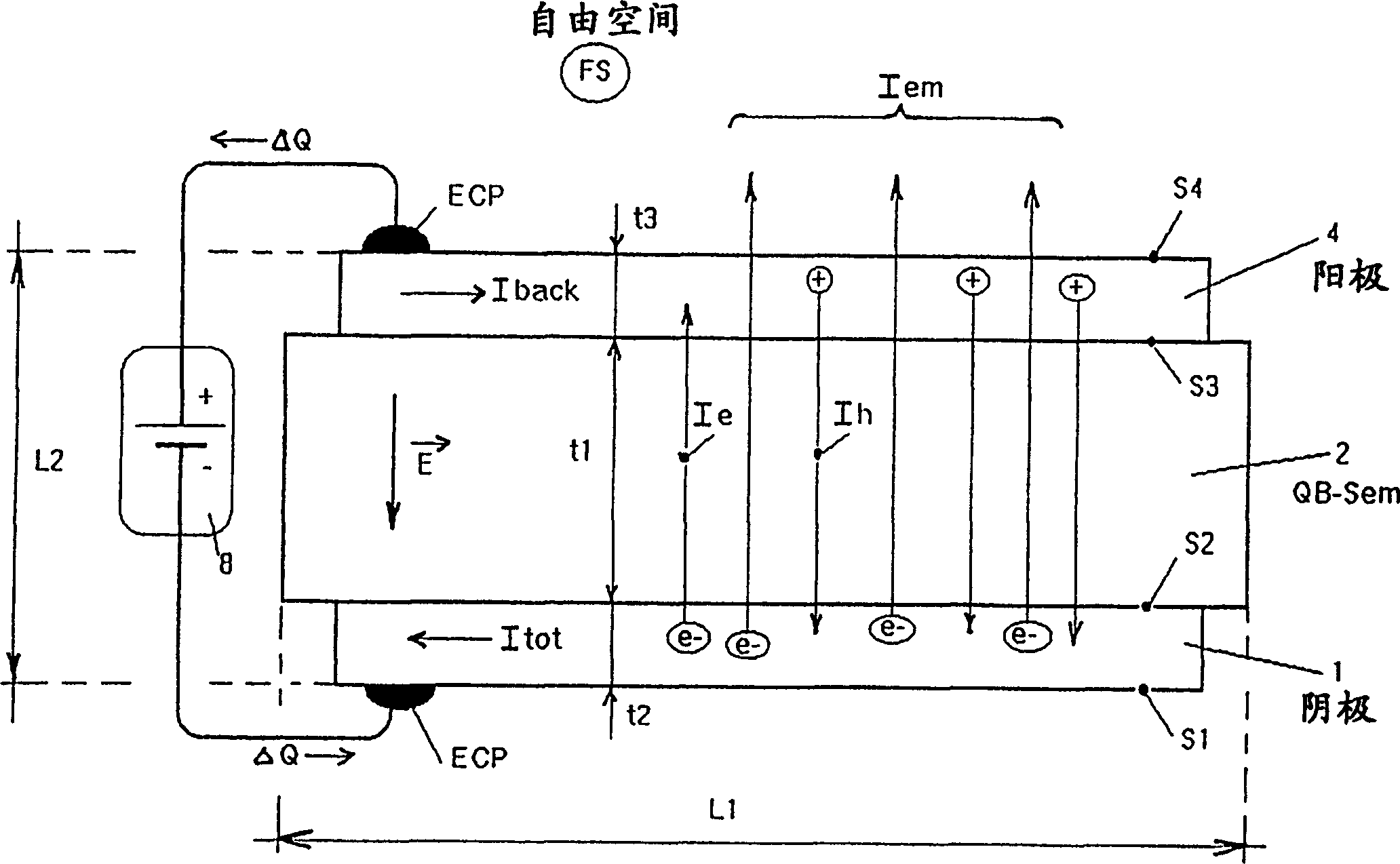
[0230] Figure 4 , that is along Figure 5 The cross-sectional view of the FE-FPD shown in , is one of the possible vacuumless FE-FPDs according to the present invention. see image 3 , the basic planar structure of the present invention-1 (cathode), 2 (QB-Sem) and 4 (anode-be light transparent in this preferred embodiment) in Figure 4 is also clearly shown. The only difference is that in this flat panel display application of the invention the cathode and anode are patterned and an additional thin layer 3 is introduced between the surface S3 of the QB semiconductor and the anode 4 . This third thin layer includes optional (patterned) red 5, yellow 18 and blue 11 segments formed from phosphors or other colored light emitters. The se...

example 2

[0238] Example 2. Planar Electron Beam Lithography

[0239] The main disadvantages caused by the short lifetime of prior art planar electron emitters are solved by using the planar electron emitter according to the invention. The invention provides a qualitatively novel and robust solution to the modern needs of the semiconductor industry. This method and example are shown in Figures 9 to 14 middle.

[0240] In the prior art, the used Figure 8 A schematic diagram of the principle of planar electron beam lithography is depicted. In the prior art section, a projection system for electron lithography has been described using a prior art planar electron emitter. The planar electron emitters of the present invention can be directly implemented in place of prior art emitters.

[0241] A possible embodiment of such a planar electron emitter structure according to the invention is shown in Figure 10 middle. It is the same as existing technology Figure 8 The main difference...

example 3

[0246] Example 3. Two-dimensional lighting board

[0247] Due to the simple structure, robustness, low power consumption, low operating temperature and two-dimensional nature of the planar electron emitter according to the present invention, the planar electron emitter can be conveniently used as a two-dimensional (planar and non-planar) illumination source .

[0248] One such possible lighting panel is schematically shown at Figure 15 and 16 middle. Here the basic structure of the planar electron emitter (the cathode 1, the QB semiconductor 2 and the anode 4 are used as a planar electron source (when a suitable voltage is applied between the cathode and the anode) to inject electrons into the free space FS). These electrons are accelerated by the accelerating electrode 7 in free space and enter the light emitting layer 3 . An optically transparent plate 13 , usually a glass plate, which enables the escape of the generated light energy from the structure (together with pl...


PUM


Abstract

A planar electron emitter, based on the existence of quasi-ballistic transport of electrons is disclosed. In its preferred embodiment the planar electron emitter structure consists of a body of finite gap pure semiconductor or insulator, the said body of macroscopic thickness (~1 mm) being terminated by two parallel surfaces and of a set of two electrodes deposited / grown on the said two free surfaces such that when a low external electrical field (~100 V / cm) is applied to this structure, consisting of two electrodes and the said semiconductor or insulating body sandwiched between them, a large fraction of electrons injected into the said semiconductor or insulator body from the negatively charged electrode (cathode) is quasi-ballistic in nature, that is this fraction of injected electrons is accelerated within the said semiconductor or insulator body without suffering any appreciable inelastic energy losses, thereby achieving sufficient energy and appropriate momentum at the positively charged electrode (anode) to be able to traverse through the said anode and to escape from the said structure into empty space (vacuum), said semiconductor or insulator body comprises a material or material system having a predetermined crystal orientation.

Description

technical field [0001] The present invention relates to a new method of generating and conducting quasi-ballistic electrons using semiconductor or insulator substrates when exposed to low electric fields. This approach would make it possible to accelerate electrons within the semiconductor or insulator without suffering any appreciable inelastic energy loss. Its main examples will be planar electron emitters, eg in flat panel displays and planar electron beam lithography. Background technique [0002] A number of devices using the (disclosed) planar electron emitters in various fields of application are also disclosed, and priority is also claimed for said devices. [0003] The present invention relates to the quasi-ballistic transport of electrons in high resistance semiconductors or insulators when exposed to low electric fields (approximately 100 V / cm). Quasi-ballistic transport means that electron scattering is minimized so that the electron mean free path becomes visi...

Claims


Application Information

Patent Timeline
Patent Type & Authority Patents(China)
IPC IPC(8): H01J1/30H01L29/76H01J9/02H01J1/304H01J1/312H01J29/04H01J29/10H01J29/44H01J31/12H01J37/073H01J63/06H01J63/08H01L31/10H01L33/00H01L33/02
CPCB82Y10/00H01J1/312H01J35/065H01J2235/062H01J1/30
Inventor 彼得·维斯科尔尼尔斯·奥勒·尼尔森阿明·德隆弗拉迪米尔·科拉里克
Owner 彼得・维斯科尔
Why Eureka
Try Eureka