Torque mirror driver of micro electromechanical system, producing method and use
A technology of micro-electro-mechanical systems and manufacturing methods, applied in the direction of generators/motors, relays, electromagnetic relays, etc., can solve the problems of increasing the difficulty of manufacturing processes, large polarization-related losses, and increased power consumption of devices, achieving high reliability, Effect of low optical insertion loss and low driving voltage
- Summary
- Abstract
- Description
- Claims
- Application Information
AI Technical Summary
Problems solved by technology
Method used
Image

Examples
Embodiment Construction
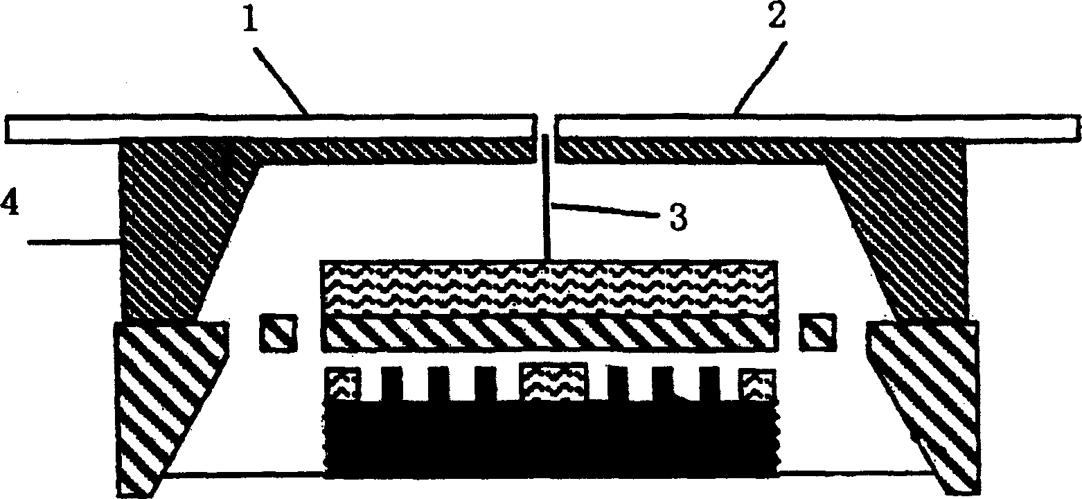
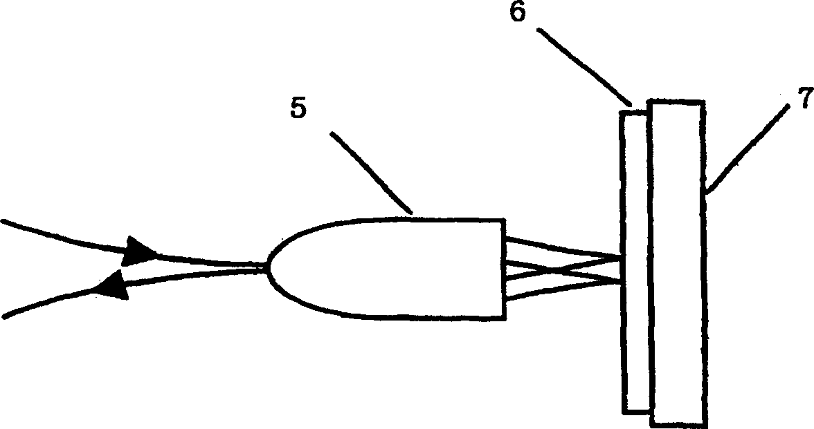
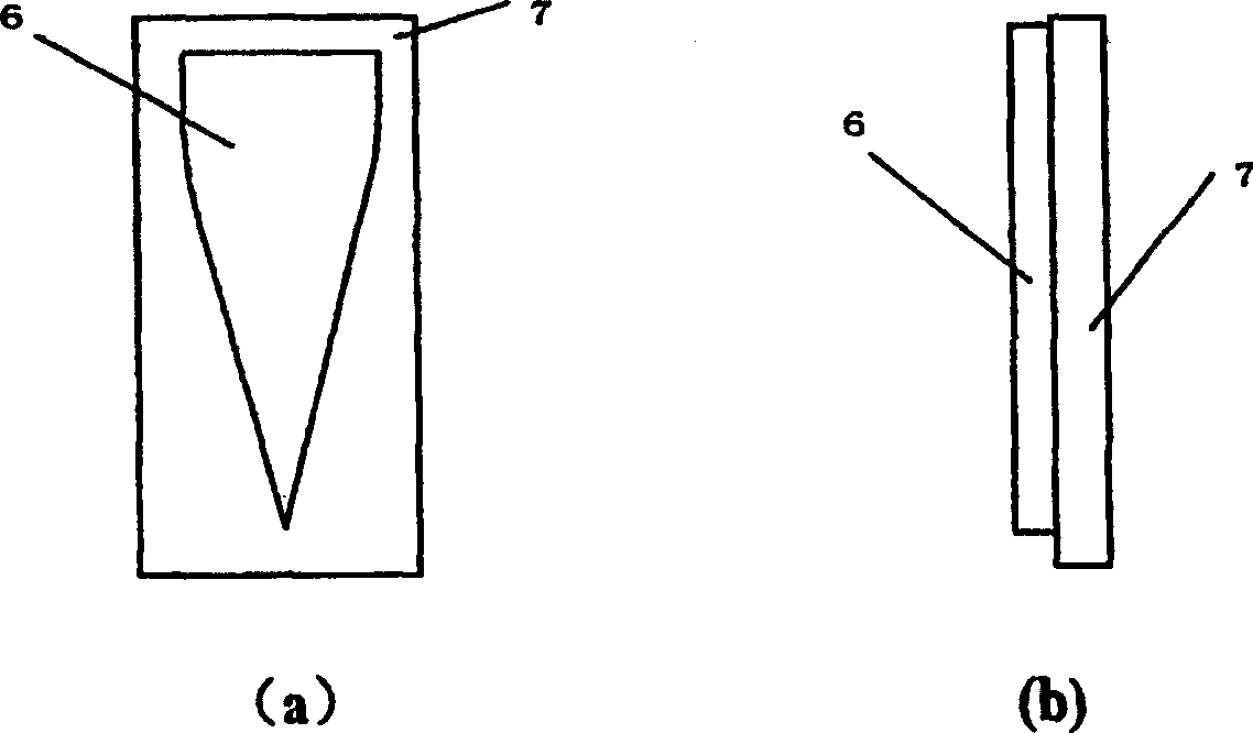
[0033] The manufacturing process steps of the MEMS twisted mirror provided by the present invention will be further explained below in conjunction with the accompanying drawings, so as to describe the specific structure of the twisted mirror driver provided by the present invention and its application as an adjustable optical attenuator.
[0034] Concrete implementation steps of the present invention are as follows:
[0035] 1. A silicon dioxide film with a thickness of about 1000 angstroms to 5000 angstroms is grown on the upper surface and the back side of the silicon wafer. Such as Figure 4 (b) shown.
[0036] 2. Use the photolithography, development and silicon dioxide etching process in MEMS technology to make the desired pattern on the silicon dioxide film. Such as Figure 4 (c) shown.
[0037]3. Put the silicon chip into the potassium hydroxide solution or TMAH solution with a solution concentration of 40% and a temperature of 40°C. The pattern on the back of the s...
PUM
 Abstract
Description
Claims
Application Information
PatSnap Eureka turns technology decisions into work you can execute. Powered by our Innovation Knowledge Graph, it runs expert workflows across engineering, life sciences, materials and intellectual property. Get your review-ready output in minutes.


