Bending cantilever beam executor and its making process
A technology of cantilever beams and actuators, applied in piezoelectric devices/electrostrictive devices, piezoelectric/electrostrictive/magnetostrictive devices, electrical components, etc., can solve the problem of high driving voltage, high cost, complex structure, etc. problems, to achieve the effect of strong adaptability, low driving voltage, and reduced energy consumption
- Summary
- Abstract
- Description
- Claims
- Application Information
AI Technical Summary
Problems solved by technology
Method used
Image
Examples
Embodiment 1
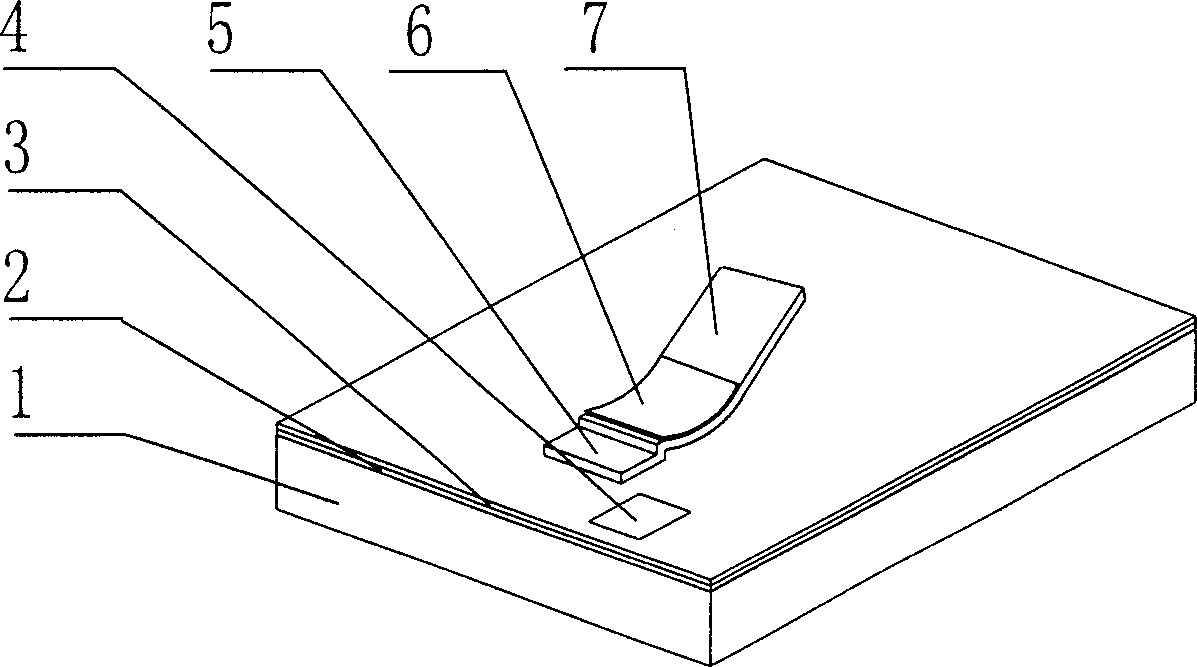
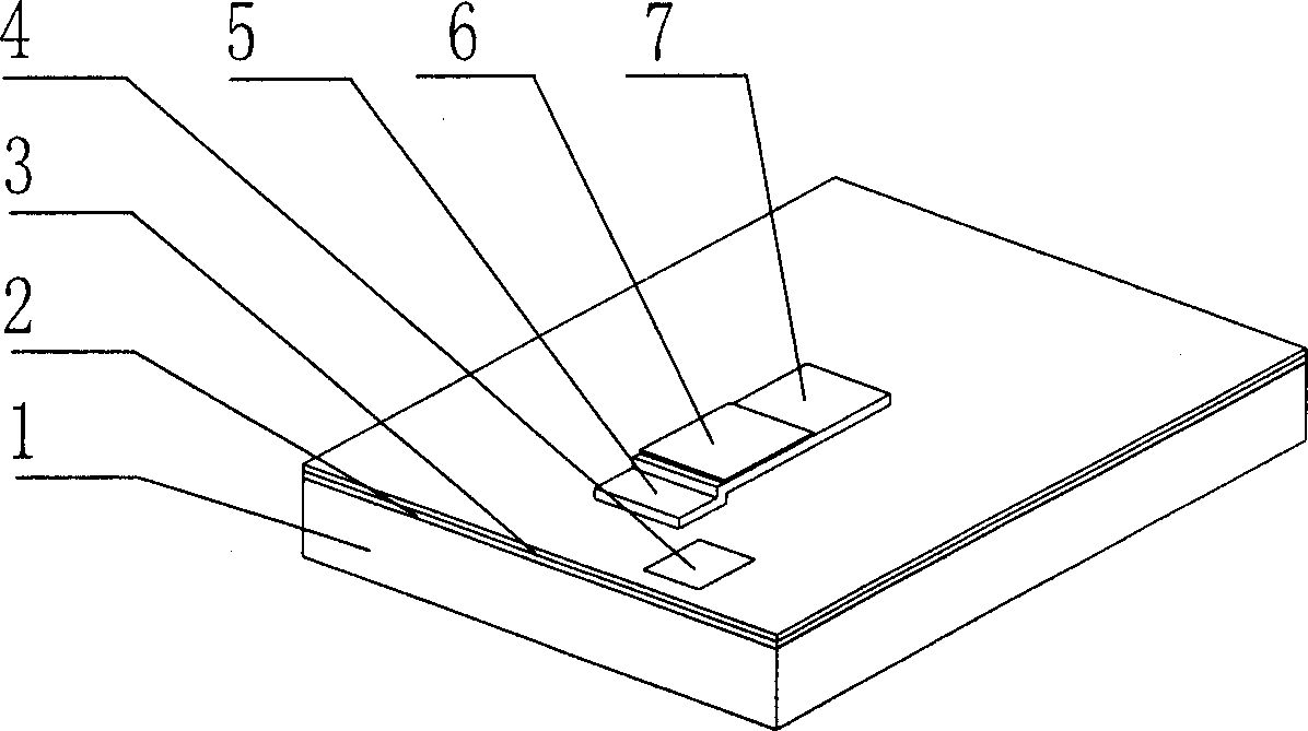
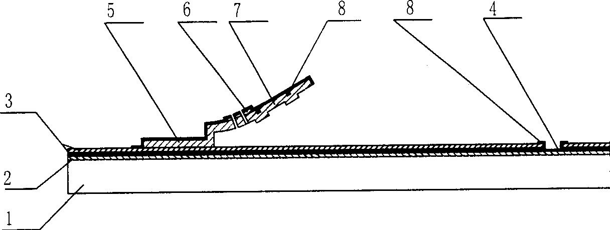
[0030] The present invention proposes a structure and manufacturing method of a curved cantilever beam actuator, and its embodiment 1 is characterized in that:
[0031] 1) heavily doping boron on the silicon wafer as the lower electrode;
[0032] 2) Depositing silicon dioxide and silicon nitride as an insulating dielectric film;
[0033] 3) Deposit a layer of phosphosilicate glass by low-pressure chemical vapor phase (LPCVD), photolithography and corrosion to form a concave column pattern for preventing the composite microbeam from adhering to the silicon substrate, and then pattern the phosphosilicate glass as a sacrificial layer ;
[0034] 4) Deposit a layer of polysilicon by low-pressure chemical vapor phase method (LPCVD), control the deposition conditions and annealing temperature process parameters, so that the polysilicon has a residual stress of -100Mpa; photolithography, etching, and cantilever beam structure;
[0035] 5) A layer of silicon nitride is deposited by l...
Embodiment 2
[0040] The present invention proposes a structure and manufacturing method of a curved cantilever beam actuator, and its embodiment 2 is characterized in that:
[0041] 1) heavily doping boron on the silicon wafer as the lower electrode;
[0042] 2) Depositing silicon dioxide and silicon nitride as an insulating dielectric film;
[0043] 3) Depositing a layer of phosphosilicate glass as a sacrificial layer by low-pressure chemical vapor method (LPCVD), photolithography and etching to form a concave column pattern for preventing the composite microbeam from adhering to the silicon substrate;
[0044] 4) Deposit a layer of polysilicon by low-pressure chemical vapor phase (LPCVD), control the deposition conditions and annealing temperature process parameters, so that the polysilicon has a residual tensile stress of 50Mpa; photolithography, etching, and cantilever beam structure;
[0045] 5) A layer of silicon nitride is deposited by low-pressure chemical vapor phase (LPCVD), and t...
Embodiment 3
[0050] Figure 4a , Figure 4b It shows a schematic diagram of using the present invention to drive an optical switch to realize optical path switching, wherein 12 is an optical fiber groove; 8, 13 are incident optical fibers; 10, 11 are outgoing optical fibers; 9 is a micromirror. Wherein, the micromirror 9 is vertically fabricated on the surface of the curved cantilever beam, the optical fiber 8 and the optical fiber 11 are on a straight line, the optical fiber 10 and the optical fiber 13 are on the same straight line, and the four optical fibers all form 45° with the surface of the micromirror 9.
[0051] Figure 4a When no voltage is applied between the upper and lower electrodes, the curved cantilever beam and the micromirror 9 are lifted away from the silicon substrate, the distance between the free end and the silicon substrate is 220 μm, the micromirror 9 is not in the optical path, and the light is transmitted from the optical fiber 8 to the optical fiber 11, From f...
PUM
| Property | Measurement | Unit |
|---|---|---|
| Length | aaaaa | aaaaa |
Abstract
Description
Claims
Application Information


