

Method for growing GaN crystal chip and GaN crystal chip
A substrate and crystal technology, applied in the field of growing GaN crystal substrates, can solve the problems that cannot be effectively used to produce GaN substrates, etc.
- Summary
- Abstract
- Description
- Claims
- Application Information
AI Technical Summary
Problems solved by technology
Method used
Image

Examples
example 1
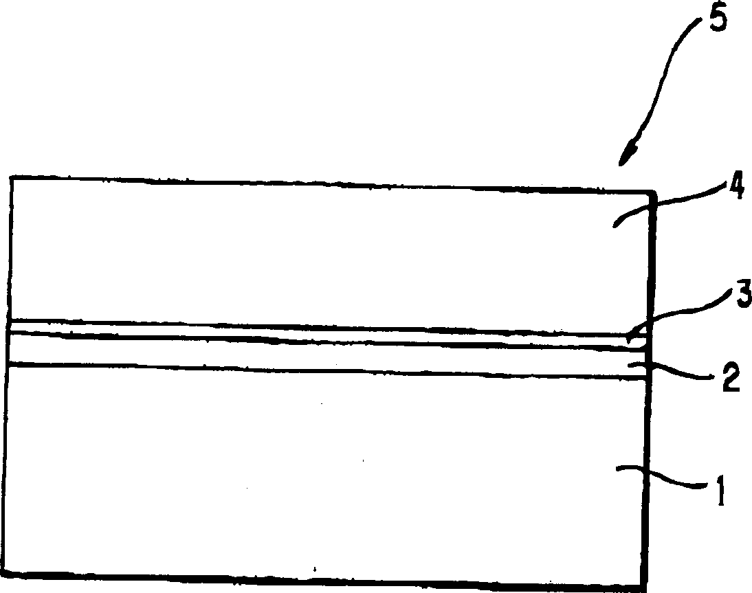
[0093] A single-crystal sapphire C-plane substrate with a diameter of 50.8 mm (about 2 inches) was used as the initial substrate, on which a 0.1 μm thick aluminum film was vapor-deposited to form a metal film. The substrate on which the aluminum film was deposited was analyzed by X-ray diffraction. As a result, not only the (0001) diffraction peak of sapphire but also the (111) diffraction peak of aluminum was observed, from which it can be confirmed that the aluminum film is C-axis oriented.
[0094] This substrate was placed in an MOCVD furnace (not shown) and heated at 650° C. for 30 minutes in a hydrogen atmosphere to clean the surface of the substrate and, at the same time, increase the degree of Al orientation. Then, in the same furnace at 650° C., a 0.1 μm-thick aluminum nitride film was grown on the surface of the aluminum film using TMA (trimethylaluminum trimethylaluminum) and ammonia as starting materials. Finally, the temperature of the substrate was raised to 105...
example 2
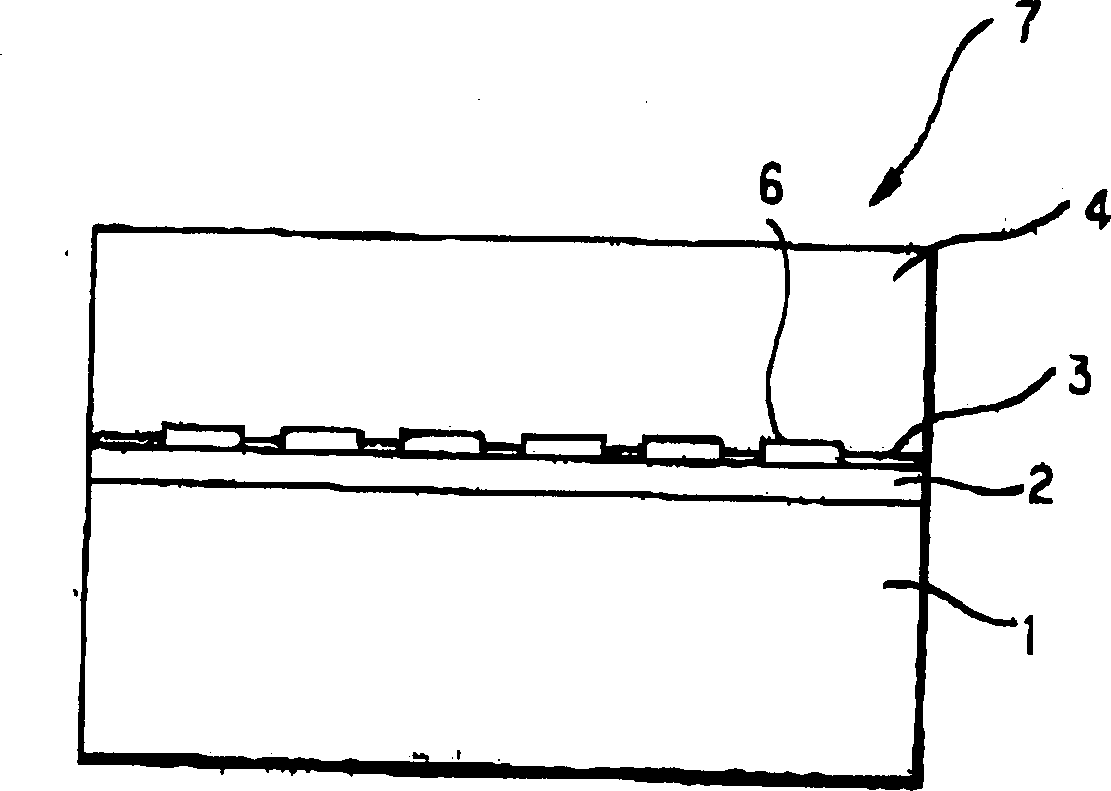
[0101] A single-crystal sapphire C-plane substrate with a diameter of 50.8 mm (about 2 inches) was placed in an MOCVD furnace as an initial substrate, and a GaN film with a thickness of 50 nm was grown at 600 °C with TMG and ammonia as initial materials. Thereafter, the temperature of the substrate was raised to 1050°C, and then the GaN film was grown to 1 µm.
[0102] A 0.1 μm-thick layer of gold was vapor-deposited on this substrate as a metal film, which was then analyzed by X-ray diffraction. As a result, (111) diffraction of the gold film was observed. This confirms that the gold film is C-axis oriented.
[0103]This substrate is again put into the MOCVD furnace. A 0.1 μm thick aluminum nitride film was grown in a furnace using TMA and ammonia as initial materials at a substrate temperature of 850°C. Then the substrate temperature was further raised to 1050°C, and the initial materials were changed to TMG and ammonia, and then a GaN film with a thickness of 2 μm was gr...
example 3
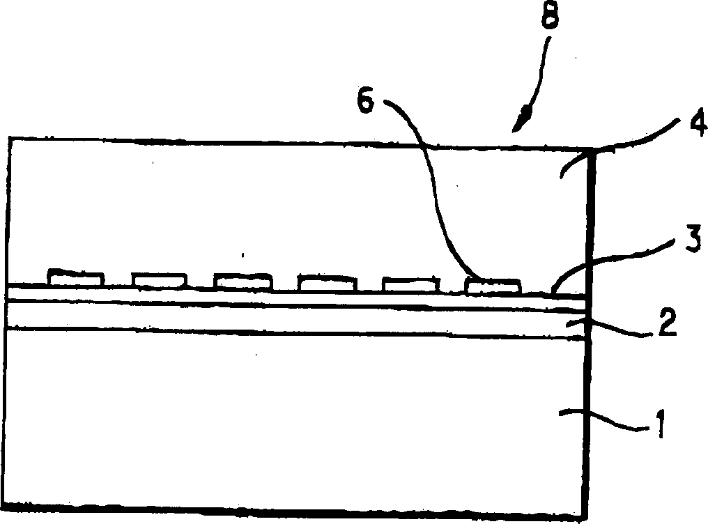
[0106] A single crystal sapphire C-plane substrate with a diameter of 50.8 mm (approximately 2 inches) was used as the initial substrate. Using the method of sputtering, 200nm thick silver is deposited on the substrate as a metal film. Then put the substrate into the MOCVD furnace, use TMG and ammonia as initial materials, and grow a GaN film with a thickness of 50nm on the surface of the silver film when the substrate temperature is 600°C. Then, the temperature of the substrate was raised to 1050°C, and a GaN film with a thickness of 1 µm was grown using TMG and ammonia as initial materials.
[0107] The substrate was then transferred to a HVPE furnace, where GaN was deposited to a thickness of 300 μm on the substrate surface. Here, ammonia and gallium chloride were used as starting materials for growth. The growth conditions were: pressure=atmospheric pressure, substrate temperature=1050°C, and growth rate=80 μm / hr.
[0108] The layered substrate obtained in this way was ...
PUM
| Property | Measurement | Unit |
|---|---|---|
| thickness | aaaaa | aaaaa |
| thickness | aaaaa | aaaaa |
| thickness | aaaaa | aaaaa |
Abstract
Description
Claims
Application Information