Conductive paste, lamina ceramic electronic element producing method and lamina ceramic electronic element
A technology of ceramic electronic components and conductivity, which is applied in the field of laminated ceramic electronic components, and can solve problems such as inability to obtain electrostatic capacity, difficult bonding, and difficult solder connection of sintered electrodes.
- Summary
- Abstract
- Description
- Claims
- Application Information
AI Technical Summary
Problems solved by technology
Method used
Image
Examples
Embodiment 1
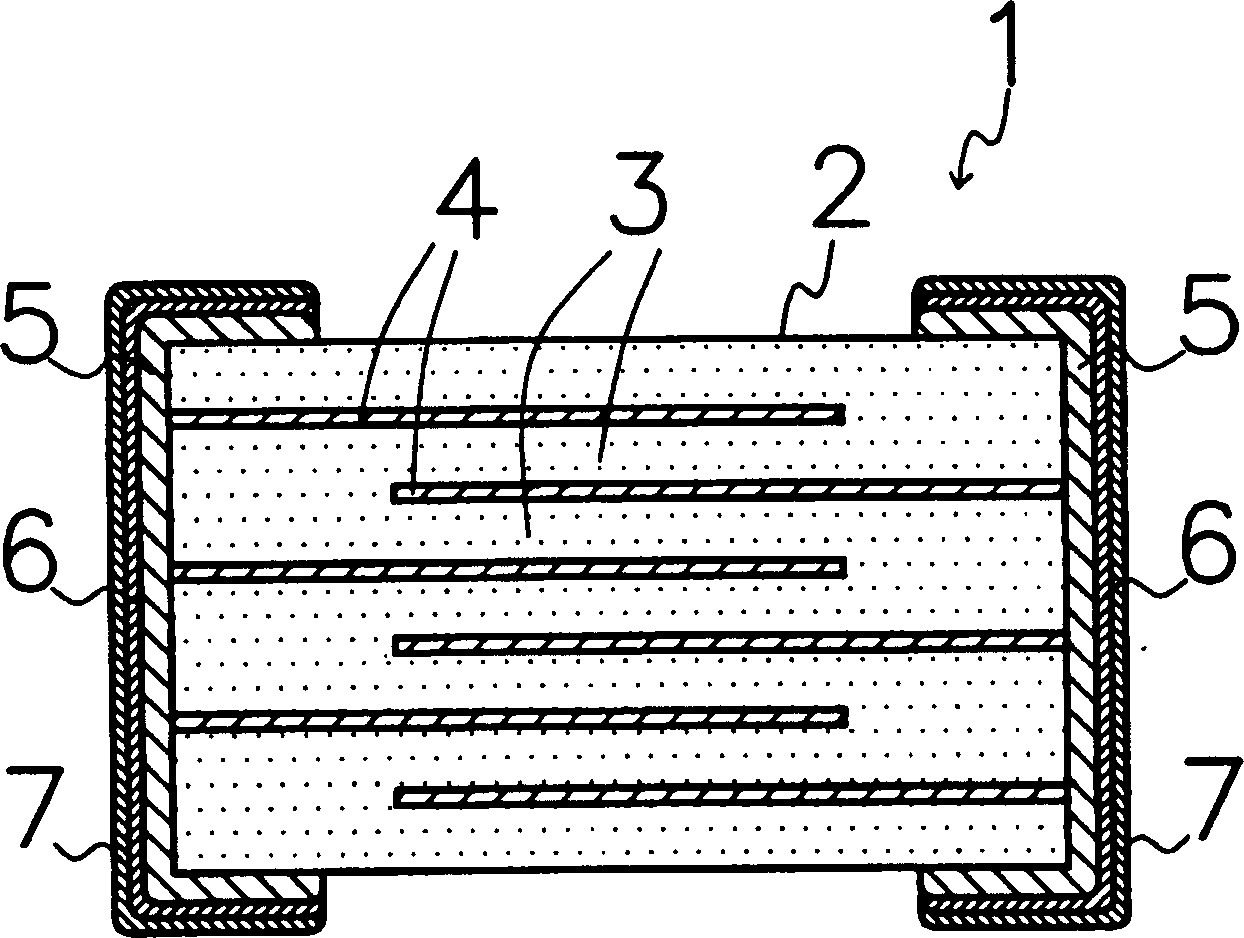
[0038] In this first embodiment, the case of a multilayer ceramic capacitor of a chip electronic component will be described.
[0039] First, as the initial raw material, weigh out the specified amount of TiCl 4 and Ba(NO 3 ), react it with oxalic acid to obtain barium titanyl oxalate (BaTiO(C 2 o 4 )·4H 2 O) precipitate, the precipitate is thermally decomposed at a temperature above 1000°C, and BaTiO is synthesized as the main component 3 .
[0040] In addition, with 0.25Li 2 O-0.65 (0.30TiO 2 0.70SiO2 2 )-0.10Al 2 o 3(Molar ratio), the oxides, carbonates or hydroxides of each component are weighed out, mixed and pulverized to obtain a powder. The mixed powder was heated to 1500° C. in a platinum crucible, cooled rapidly, and then pulverized to obtain an oxide powder as a first subcomponent having an average particle diameter of 1 μm or less.
[0041] Then, with 0.66SiO2-0.17TiO 2 -0.15BaO-0.02MnO (molar ratio), weigh out the oxides, carbonates or hydroxides of ea...
Embodiment 2
[0052] In this second embodiment, the case of a laminated forward thermistor of a chip electronic component will be described.
[0053] First, as a raw material, in order to obtain (Ba 0.9998 SM 0.0002 )TiO 3 And weigh BaCO3, TiO 2 and Sm 2 o 3 . Pure water was added to the obtained powder, mixed and pulverized together with cobalt oxide balls in a ball mill for 16 hours, dried and then calcined at 1200° C. for 2 hours to obtain a calcined powder.
[0054] Add polyvinyl butyral as a binder and ethanol as a solvent to the calcined body obtained above, and mix in a ball mill to obtain a ceramic crystal slurry. Then, sheet forming was performed by the doctor blade method using this crystallization slurry to obtain a rectangular ceramic printed circuit board having a thickness of 35 μm.
[0055] Then, a conductive paste containing Ni as a main component was printed on the ceramic printed circuit board to form a conductive paste layer as a layer for internal conductors.
[...
PUM
| Property | Measurement | Unit |
|---|---|---|
| diameter | aaaaa | aaaaa |
| diameter | aaaaa | aaaaa |
| thickness | aaaaa | aaaaa |
Abstract
Description
Claims
Application Information

