

SiGe/Si Chemical vapor deposition growth process
A chemical vapor deposition, silicon germanium technology, applied in electrical components, semiconductor/solid-state device manufacturing, circuits, etc., can solve the problems of epitaxial material pollution, affecting the quality of epitaxial layers, low background vacuum, etc. Clear, reduce material interface unclear, improve the effect of crystal quality
- Summary
- Abstract
- Description
- Claims
- Application Information
AI Technical Summary
Problems solved by technology
Method used
Image


Examples
Embodiment Construction
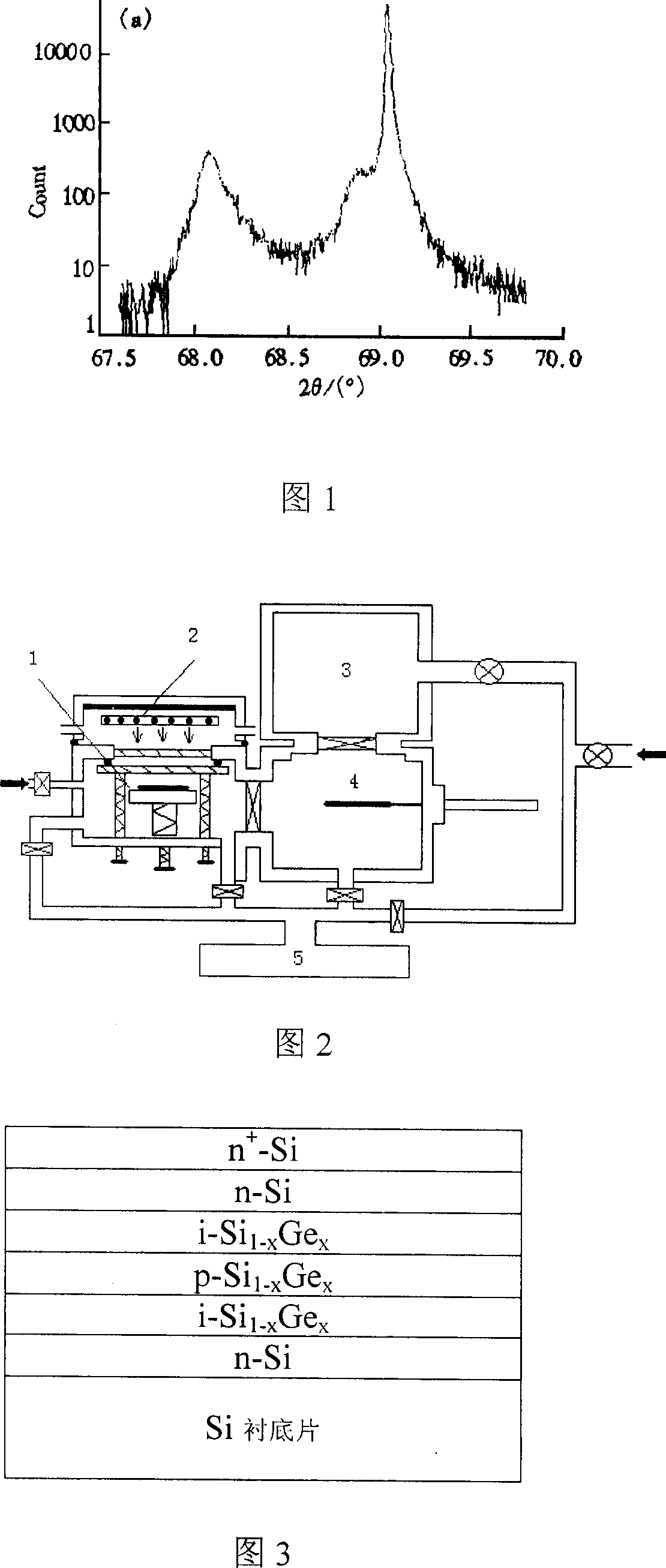
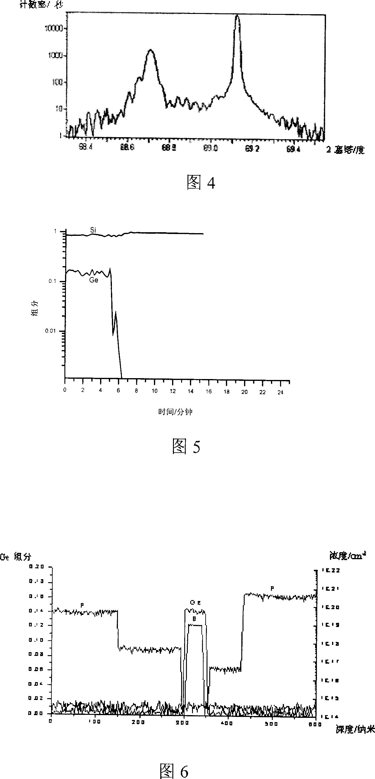
[0030] The present invention will be further described below through multiple examples realized on the novel photochemical vapor deposition equipment shown in FIG. 2 (this equipment has applied for a Chinese patent with application number 02262163.6).
[0031] Example 1 grows a layer of intrinsic silicon germanium (SiGe) on the Si substrate 1-x Ge x ) material, its technical process is carried out according to the following steps:
[0032] Step 1: filling the processing chamber of the photochemical vapor deposition equipment with high-purity nitrogen to an atmospheric pressure. After the RCA treatment, the Si substrate is quickly placed in the high-purity nitrogen-protected processing chamber 3, and the processing chamber 3 is sealed;
[0033] Step 2: In the processing chamber 3, put the Si substrate into a 10% hydrofluoric acid (HF) solution through a sealed rubber glove, take it out after 30 seconds and put it into the substrate tray; at the same time, fill up the preparat...
PUM
 Abstract
Description
Claims
Application Information