Process for preparing high polymer micro-flow control chips
A microfluidic chip and polymer technology, applied in biochemical equipment and methods, microbial determination/inspection, biological testing, etc., can solve problems such as being unsuitable for mass production, increasing production costs, and easily falling off photoresist , to achieve the effect of hard material, easy mass production and low price
- Summary
- Abstract
- Description
- Claims
- Application Information
AI Technical Summary
Problems solved by technology
Method used
Image

Examples
Embodiment 1
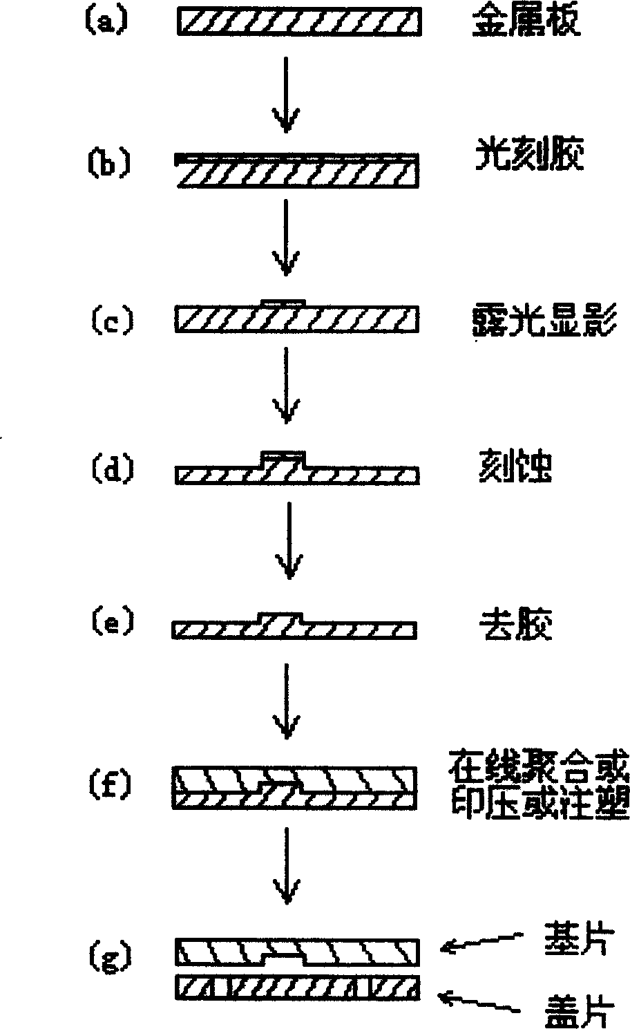
[0049] (1) Production of cover slip: Place a stainless steel column with a diameter of 2 mm and a height of 2 mm on a specific position of the smooth glass, and the mixture of PMMA monomer and benzoyl peroxide (1000:5 by weight) is pre-treated. After polymerization and degassing, it was transferred to the glass, and the air was removed and sealed. After 24 hours of low-temperature polymerization (45° C.) and two hours of high-temperature polymerization (90° C.), the peeling template was taken out at 40° C. (2) Metal negative plate production: Rinse the titanium gold plate with water, put it in a lotion for one day, remove the surface oil, rinse it with distilled water, and dry it. Spin the glue (BP-213) on the titanium plate and pre-bake it. The pre-bake time is 5 minutes and the temperature is 90 degrees. Place the mask plate with the microchannel network on the photoresist, expose it to ultraviolet light for 1 minute, and then use 0.5wt% NaOH solution to develop it at 15°C f...
Embodiment 2
[0053] (1) Production of metal negative plate: Rinse the stainless steel plate with water, put it in a lotion for one day, remove the surface oil, rinse it with distilled water, and dry it. Spin the glue (RZJ-390) on a stainless steel plate and pre-bake it. The pre-bake time is 1.5 minutes and the temperature is 100 degrees. Put the mask plate with the microchannel network pattern on the photoresist, expose it to ultraviolet light for 20 seconds, then put the metal plate in 0.4wt% NaOH solution, develop it at 25°C for 5 minutes, and remove the microchannels on the stainless steel plate. The photoresist outside the channel network is baked at 130 degrees for half an hour. The stainless steel plate was etched at 50° C. for 10 minutes with ferric chloride acidic corrosion solution, the content of ferric chloride in the corrosion solution was 25 wt %, and the corrosion solution contained 0.2 wt % of quaternary ammonium salt corrosion inhibitor. A stainless steel negative plate wi...
Embodiment 3
[0057] (1) Production of metal negative plate: Rinse the stainless steel plate with water, put it in a lotion for one day, remove the surface oil, rinse it with distilled water, and dry it. Apply glue JL-SR1000 on the stainless steel plate by screen printing technology and pre-baking. The pre-baking time is 30 minutes and the temperature is 80 degrees. Place the mask plate with the microchannel network pattern on the photoresist, expose to UV light for 20 seconds, and then put the metal plate into 0.2wt% Na 2 CO 3 In the solution, develop at 25°C for 5 minutes, remove the photoresist outside the microchannel network on the stainless steel plate, and bake at 120°C for 15 minutes. The stainless steel plate was etched at 50° C. for 10 minutes with ferric chloride acidic corrosion solution, the content of ferric chloride in the corrosion solution was 25 wt %, and the corrosion solution contained 0.2 wt % of quaternary ammonium salt corrosion inhibitor. A stainless steel negative...
PUM
| Property | Measurement | Unit |
|---|---|---|
| Depth | aaaaa | aaaaa |
| Width | aaaaa | aaaaa |
| Thickness | aaaaa | aaaaa |
Abstract
Description
Claims
Application Information
PatSnap Eureka turns technology decisions into work you can execute. Powered by our Innovation Knowledge Graph, it runs expert workflows across engineering, life sciences, materials and intellectual property. Get your review-ready output in minutes.


