Single electron trivalue storage based on coulomb baffle principle design and its preparation method

A principle design, Coulomb blocking technology, applied in the direction of electric solid devices, circuits, electrical components, etc., to achieve the effect of high storage density, enhanced storage time, and simple structure

Inactive Publication Date: 2004-05-05
INST OF PHYSICS - CHINESE ACAD OF SCI
View PDF0 Cites 0 Cited by
  • Summary
  • Abstract
  • Description
  • Claims
  • Application Information

AI Technical Summary

Problems solved by technology

Because traditional CMOS has only two states: on and off, traditional CMOS-based memory cells are limited in many ways when performing multi-value storage

Method used


Image

  • Single electron trivalue storage based on coulomb baffle principle design and its preparation method
  • Single electron trivalue storage based on coulomb baffle principle design and its preparation method
  • Single electron trivalue storage based on coulomb baffle principle design and its preparation method

Examples


Embodiment 1

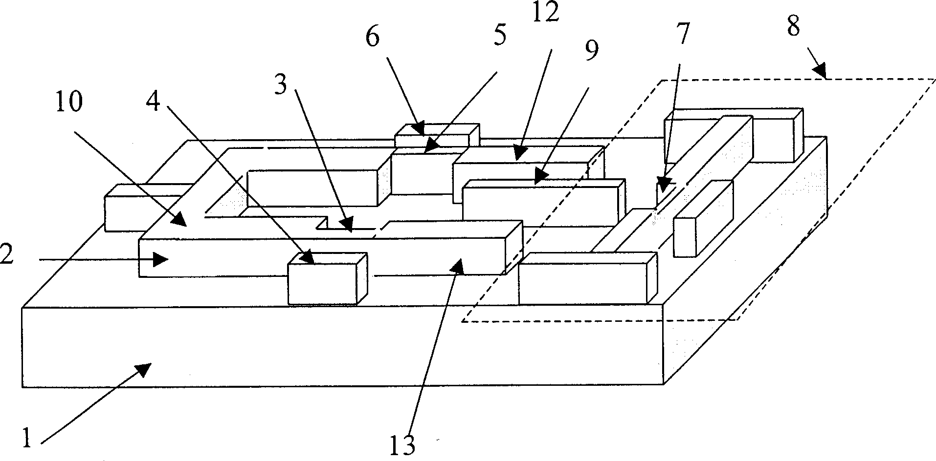
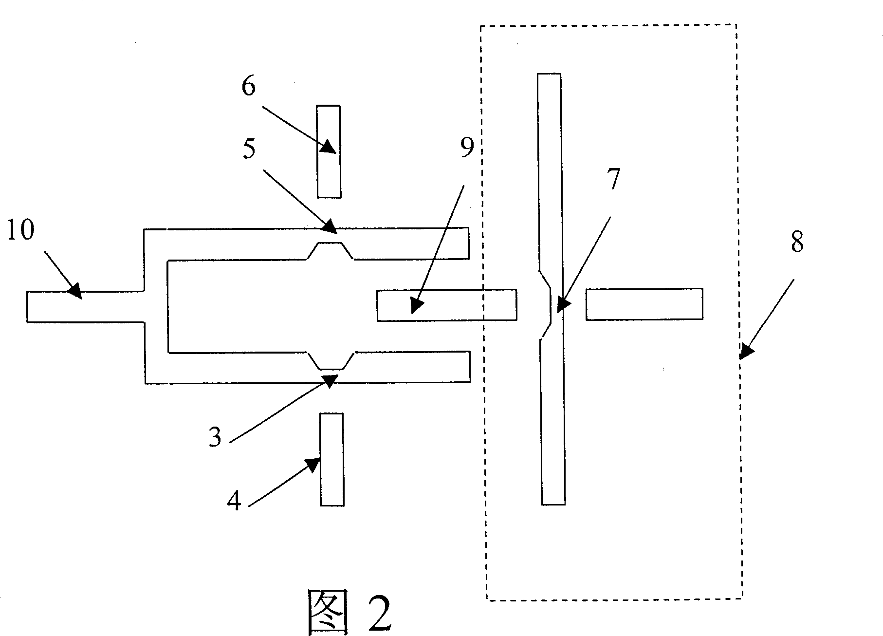
[0036] according to figure 1 and 2 make a single-electron ternary memory designed based on the Coulomb blocking principle of the present invention, and the present invention will be described in detail below in conjunction with embodiments and manufacturing methods:

[0037] A half-insulating GaAs sheet is selected, and a 1-micron-thick GaAs buffer layer is grown on it by molecular beam epitaxy (MBE) to form an insulating substrate 1 . A silicon delta-doped GaAs layer is formed on the buffer layer by molecular beam epitaxy, and the layer is deposited on the GaAs buffer layer with an area density of 1×10 12 cm -2 Silicon and a 50nm-thick GaAs layer grown on it, which constitutes the conductive material layer 2 of the device.

[0038] Then, the following structures (such as figure 1Shown): the first side gate 4, the second side gate 6, the gate length is 200 nanometers, the length of the two depleted nanowires is 200 nanometers, the width is 100 nanometers, and the distance b...

Embodiment 2

[0040] Silicon with (001) orientation is selected, and a 60 nm thick silicon dioxide insulating layer is oxidized by dry oxygen oxidation method at an oxidation temperature of 900° C., which forms the substrate 1 . A 40nm-thick polysilicon layer is formed on the oxide layer by molecular beam epitaxy MBE or chemical vapor deposition, and heavily doped with arsenic to become an n-type semiconductor layer with an implantation dose of 6×10 13 cm -2 , so that the highly doped silicon layer forms the conductive material layer 2 .

[0041] The preparation of other parts of the device is the same as in Example 1.

Embodiment 3

[0043] Silicon on insulator (SOI) is selected, which is prepared by oxygen injection isolation process, and the top layer silicon is thinned by dry oxygen oxidation. The parameters are as follows: material crystal orientation , P type, resistivity 3Ωcm; thickness of top layer silicon is 40 nm, and the thickness of the buried silicon dioxide is 200 nm. The n-type conductive layer is formed by implanting impurity arsenic into the thinned top silicon, and the implantation dose is 5×10 13 cm -2 . The doped top layer silicon is thinned to form the conductive material layer 2 .

[0044] The preparation of other parts of the device is the same as in Example 1.


PUM


Abstract

The storage device possesses an insulative base plate with a conducting material layer on it. There are two structures of multiple tunneling junctions, one single electron transistor and one storage junction unit. One end of two tunneling junctions through lead wire connected to each other is as input end for writing in voltage, and the other end of each tunneling junction is connected to a storage junction. Middle capacitance in storage junction unit is coupled each other. Single electron transistor possesses source pole, drain pole, quantum point weak coupled to source/drain pole and grid pole for controlling static chemical potential energy of quantum point. Quantum point is connected to storage junction unit through mode of capacitance coupling. The part possesses three stable store statuses. Only controlling movement of minute electron can implement normal operation of the part so as to realize storing information in super high density under low power consumption.

Description

technical field [0001] The invention belongs to a single-electron multi-value memory device, in particular to a single-electron multi-value memory with three stable storage states designed by utilizing the Coulomb blocking effect of a multi-tunnel junction structure and a preparation method thereof. Background technique [0002] Memory accounts for 40% of the world's semiconductor market. Semiconductor products other than memory are updated every 2 years, while memory is a generation every 18 months. Taking the development of dynamic memory (DRAM) as an example, in 1988 Japan The line width of the lines on the silicon chip reached 0.8 microns, and the 4Mb DRAM came out, thus entering the era of ultra-large-scale integration ULSI; in 1992, the 16Mb chip with a line width of 0.5 microns was put into production; in 1994, the 64Mb chip with a line width of 0.35 microns was launched. Chip production; 0.13-micron 4Gb DRAM will soon be realized. However, maintaining the trend of c...

Claims


Application Information

Patent Timeline
Patent Type & Authority Applications(China)
IPC IPC(8): H01L27/00
Inventor 孙劲鹏王太宏
Owner INST OF PHYSICS - CHINESE ACAD OF SCI
Why Eureka
Try Eureka