

Magnetically controlled sputtering process of making printed circuit board
A printed circuit board, magnetron sputtering technology, applied in the direction of printed circuit, printed circuit manufacturing, and the formation of electrical connection of printed components, can solve problems such as connection conduction, improve efficiency, reduce pollution, and avoid uneven coating. Effect
- Summary
- Abstract
- Description
- Claims
- Application Information
AI Technical Summary
Problems solved by technology
Method used
Image

Examples
specific Embodiment 1
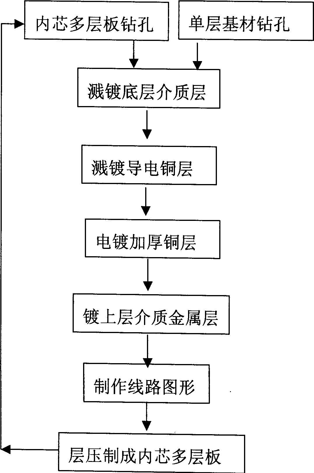
[0019] Specific embodiment one: make multi-layer printed circuit board, adopt whole board electroplating technology, its production process is as follows figure 2 Shown:
[0020] 1) Drilling: After cleaning the board to be operated, drill through holes on the board to be operated according to the design requirements of the circuit board.
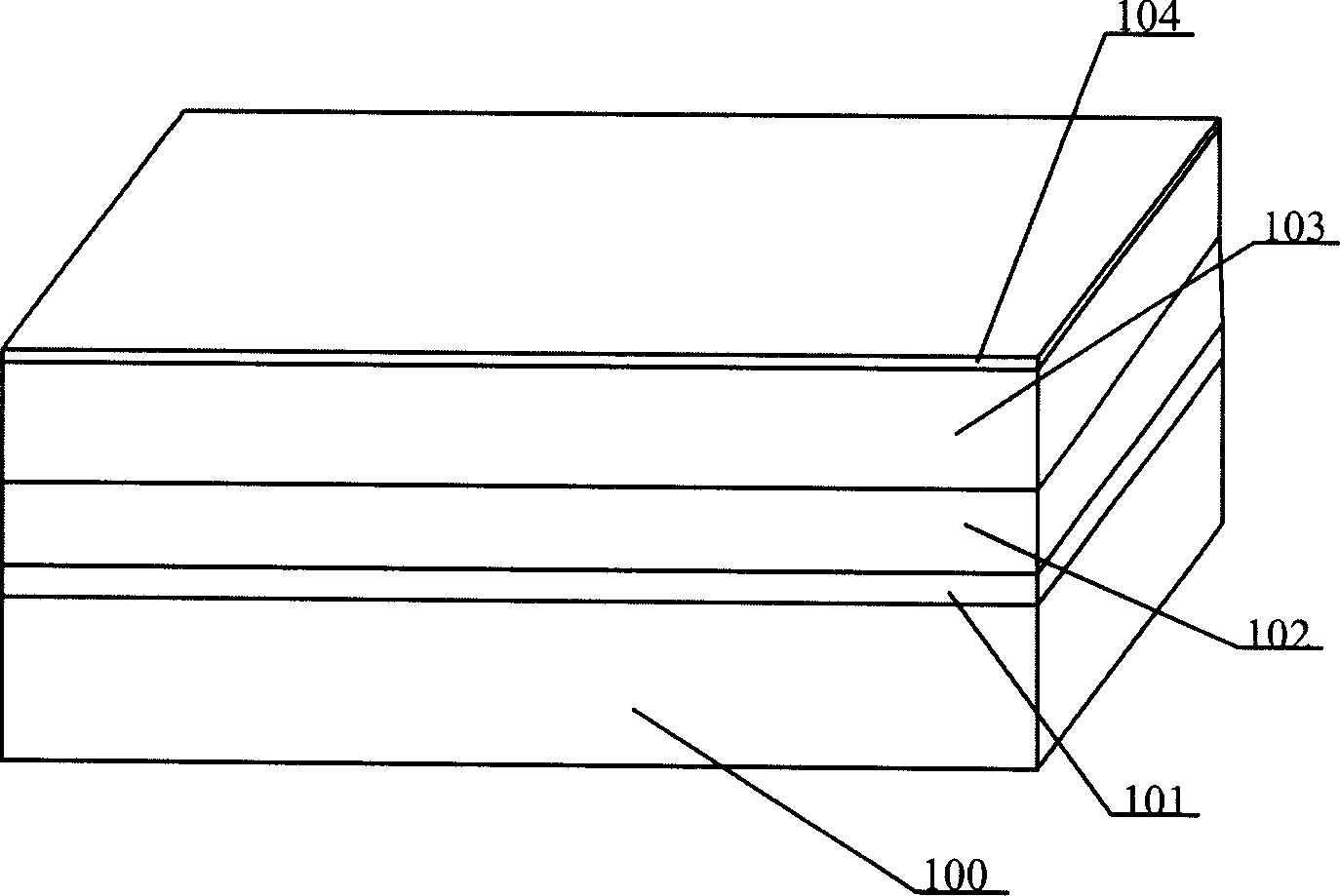
[0021] 2) After the drilled plate is cleaned, chromium, nickel and nickel-copper alloy are sequentially sputtered on the surface of one side or both sides of the plate and the inner wall of the hole to improve the affinity between the copper foil and the substrate , the sputtering time is set to 0.1-5min according to the thickness of the coating, the sputtering current should not be too small to avoid low efficiency, it is set to 0.1-5A, the sputtering gas pressure is -3 to 3×10 -3 torr;
[0022]3) Sputter a conductive copper layer of 0.1-5 μm on the surface of one side or both sides of the plate to be operated and the dielectric layer me...
specific Embodiment 2
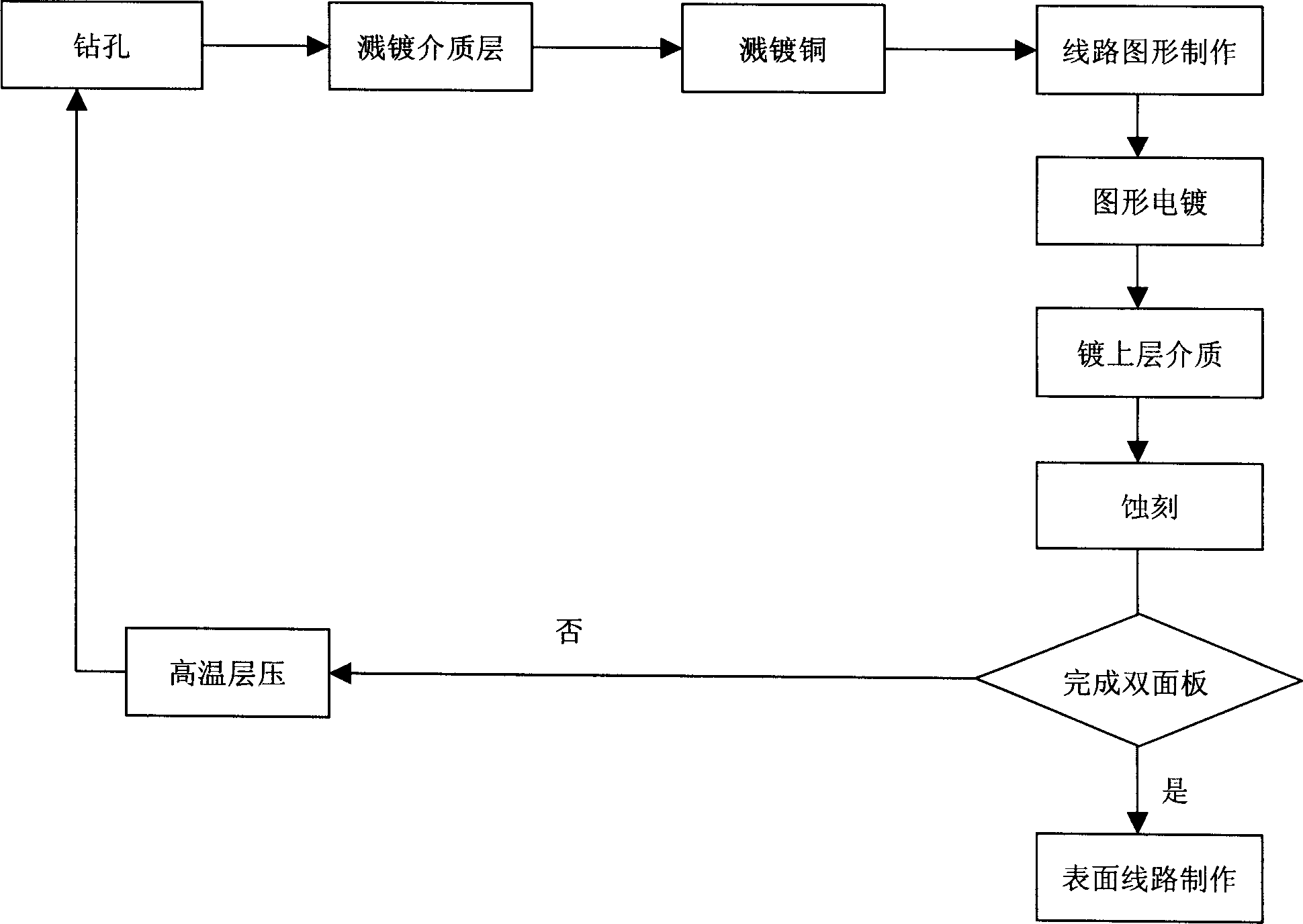
[0037] Specific embodiment two: make double-sided printed circuit board, use graphic electroplating technology, its production process is as follows figure 2 Shown:
[0038] 1) Drilling: After cleaning the board to be operated, drill through holes on the board to be operated according to the design requirements of the circuit board.
[0039] 2) Clean the single-layer substrate after drilling, and magnetron sputtering on the surface of one side or both sides and the inner wall of the hole to improve the affinity between the copper foil and the substrate. The underlying dielectric metal layer, technical and process requirements With embodiment one;
[0040] 3) Magnetron sputtering a conductive copper layer on the surface of one side or both sides of the single-layer substrate and the dielectric layer metal on the inner wall of the hole, the technical and process requirements are the same as those in Embodiment 1;
[0041] 4) Line graphics production. Paste the photosensitive...
specific Embodiment 3
[0049] Specific embodiment three: make multi-layer printed circuit board, circuit forming uses floating technology, and its production process is as follows Figure 4 Shown:
[0050] 1) Drilling: After cleaning the substrate board to be operated, drill holes on the board to be operated according to the design requirements of the circuit board;
[0051] 2) Clean the substrate.
[0052] 3) Making a negative image of the circuit: coating or pasting a layer of photosensitive material on the surface of the substrate, exposing and developing the substrate on a photolithography machine, cleaning the surface of the substrate to obtain a negative image of the circuit coated with photosensitive material, and then drying ;
[0053] 4) Sputtering medium layer: After the drilled plate is cleaned, three metals such as chromium, nickel and nickel-copper alloy are sequentially sputtered on the surface of one side or both sides of the plate and the inner wall of the hole. Adhesive layer, te...
PUM
| Property | Measurement | Unit |
|---|---|---|
| Peel strength | aaaaa | aaaaa |
| Thickness | aaaaa | aaaaa |
Abstract
Description
Claims
Application Information