
Method for fabricating ferroelectric random access memory device

A technology of random access memory and manufacturing method, applied in static memory, digital memory information, capacitors, etc., can solve the problems of oxygen diffusion, oxidation of titanium nitride layer, increase of leakage current, etc.

Inactive Publication Date: 2004-09-29
SK HYNIX INC
View PDF0 Cites 4 Cited by
  • Summary
  • Abstract
  • Description
  • Claims
  • Application Information

AI Technical Summary

Problems solved by technology

The oxide layer on the third titanium nitride layer may increase the leakage current
This leads to the easy diffusion of oxygen to the titanium nitride layer during the high-temperature crystallization heat treatment process of the ferroelectric layer, resulting in the oxidation of the titanium nitride layer.
As a result, the oxidized TiN leads to an increase in leakage current, which in turn leads to an increase in the contact resistance between the bottom electrode and the tungsten plug

Method used


Image

  • Method for fabricating ferroelectric random access memory device
  • Method for fabricating ferroelectric random access memory device
  • Method for fabricating ferroelectric random access memory device

Examples


Embodiment Construction

[0037] Hereinafter, details of preferred embodiments of the present invention will be described with reference to the accompanying drawings.

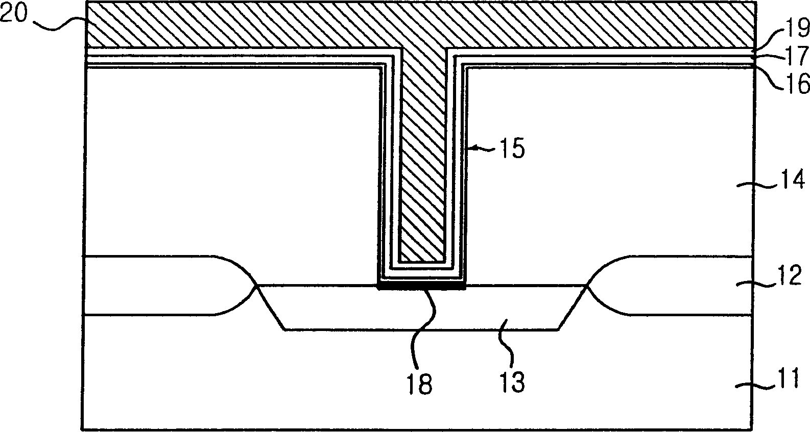
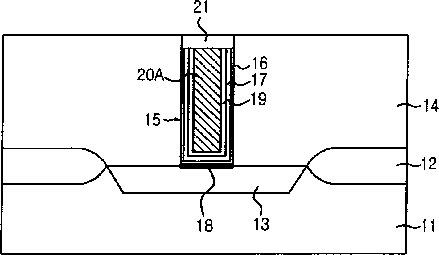
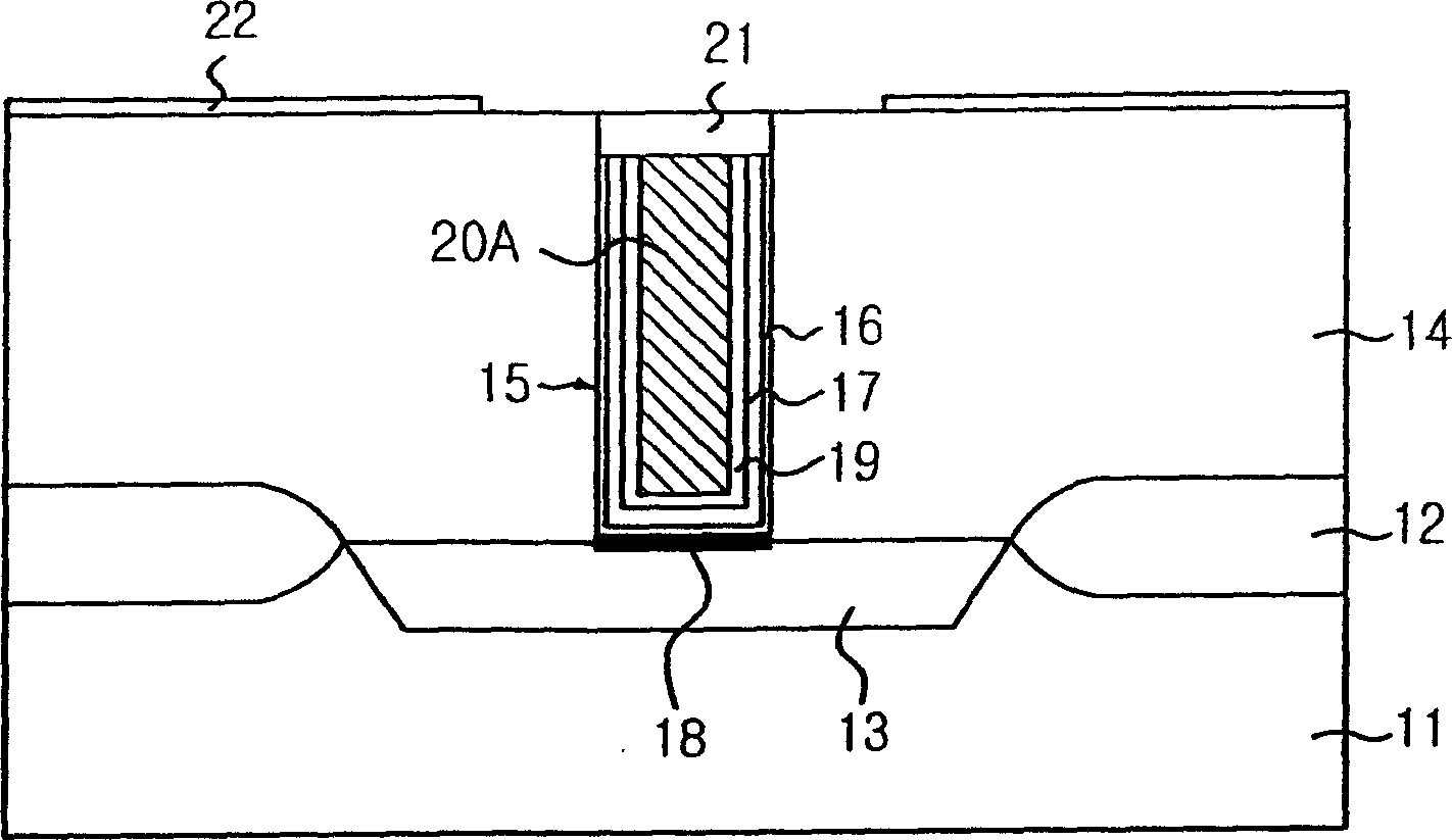
[0038] Figures 4A-4G revealed Figures 7A-7HIt is the manufacturing process of the FeRAM of the first preferred embodiment of the present invention.

[0039] refer to Figure 4A A field oxide layer 32 is grown on the substrate 31, and an impurity junction region 33, such as a source / drain region of a transistor, is formed on the substrate 31. Then, a first interlayer insulating layer 34 is grown on the substrate 31 . In this example, the first interlayer insulating layer 34 is a multi-layer structure, which can isolate the word line, ferrule plug and bit line before forming the storage node contact structure. Preferably, the first interlayer insulating layer 34 is made of silicon oxide, including high density plasma (HDP) oxide, borophosphosilicate glass (BPSG), phosphosilicate glass (PSG), medium temperature oxide (MTO) , high tem...


PUM


Abstract

The present invention relates to a method for fabricating a ferroelectric random access memory device. The method includes the steps of: (a) forming a first inter-layer insulation layer on a substrate providing a transistor; (b) etching the first inter-layer insulation layer to form a storage node contact hole exposing a partial portion of the substrate; (c) burying a storage node contact including a plug and a barrier metal layer into the storage node contact hole; (d) forming an adhesion layer on the storage node contact and the first inter-layer insulation layer; (e) inducing a predetermined portion of the adhesion layer to be cracked, the predetermined portion disposed above an upper part of the plug; (f) selectively removing the cracked predetermined portion to expose a surface of the barrier metal layer formed on the plug; and (g) forming a ferroelectric capacitor connected to the plug through the exposed surface of the barrier metal layer.

Description

technical field [0001] The invention relates to a manufacturing method of a semiconductor device, in particular to a manufacturing method of a ferroelectric random access memory (FeRAM). Background technique [0002] How to use the ferroelectric layer to form a ferroelectric capacitor to develop a large-scale semiconductor memory device and overcome the inherent refresh bottleneck of dynamic random access memory (DRAM) has always been a research hotspot. This FeRAM, made using a ferroelectric layer, is a type of non-volatile memory. This means that FeRAM has an inherent advantage of being able to read its data even when the power is turned off. At the same time, FeRAM has become the focus of attention as a candidate for next-generation memory due to its response speed comparable to that of DRAM. [0003] The upper and lower electrodes of ferroelectric capacitors generally use materials with good conductivity, such as Pt, Ir, and Ru. However, when this noble metal is used ...

Claims


Application Information

Patent Timeline
Patent Type & Authority Applications(China)
IPC IPC(8): B44C1/22G11C11/22H01L21/02H01L21/306H01L21/469H01L21/768H01L21/82
CPCH01L21/76829H01L21/76877H01L21/76828H01L21/02052H01L21/7687H01L21/76889H01L21/76834H01L21/76846H01L28/65H01L28/55
Inventor 权纯容廉胜振
Owner SK HYNIX INC
Learn More