Polarized don't-care semiconductor optical enlarger

An optical amplifier and semiconductor technology, used in semiconductor lasers, lasers, laser parts, etc., can solve the problems of leakage, poor temperature characteristics of semiconductor amplifiers, etc., to prevent leakage, reduce absorption between valence bands, and prevent electrons from crossing the barrier layer. The effect of leakage

Inactive Publication Date: 2005-01-12
HUAZHONG UNIV OF SCI & TECH
View PDF0 Cites 7 Cited by
  • Summary
  • Abstract
  • Description
  • Claims
  • Application Information

AI Technical Summary

Problems solved by technology

[0004] Most semiconductor lasers and amplifiers are temperature-sensitive devices. In the practical application of semiconductor optical amplifiers, especially in their integrated applications, good temperature characteristics are extremely important. InGaAsP-InP is currently a relatively mature semiconductor laser and amplifier materials, but semiconductor amplifiers based on InGaAsP-InP material systems have poor temperature characteristics and are subject to many restrictions in practical optical networks and device integration applications, because in quantum well structures, carriers are mainly conduction band electrons It will leak out of the active region through the barrier layer, and the probability of electrons leaking out through the barrier layer is related to the barrier height of the conduction band of the quantum well

Method used


Image

  • Polarized don't-care semiconductor optical enlarger
  • Polarized don't-care semiconductor optical enlarger
  • Polarized don't-care semiconductor optical enlarger

Examples


Embodiment Construction

[0013] The present invention will be further described in detail below with an example of a 1.55 μm polarization-independent strained quantum well semiconductor optical amplifier.

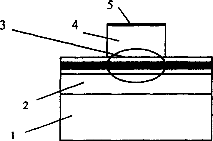
[0014] Such as figure 1 As shown, the present invention includes an InP substrate 1 , an n-type InP buffer layer 2 , a tensile strain active region 3 , a p-type ridge waveguide 4 and a p-type InGaAs contact layer 5 . Like a common optical amplifier, the top and bottom of the above-mentioned device are also provided with electrodes made of Ti / Pt / Au, which are not marked in the drawings. The active region 3 generally has three structures: A. adopting a tensile strained AlGaInAs bulk material structure, B. a tensile strained multi-quantum well structure, and C. a tensile strained barrier multi-quantum well structure.

[0015] The specific technological implementation process of the 1.55 μm polarization-independent strained quantum well semiconductor optical amplifier based on the AlGaInAs-InP materia...


PUM


Abstract

The light amplifier includes InP substrate, n type InP buffer layer, active region in tensile strain structure of quanta trap, O type InP cladding layer, P type InGaAs contact layer, and electrodes in top and bottom layers. Characters are that AlGalnAs is adopted in active region so as to prevent electrons to pass through barrier layer causing leak, and improve high temperature characteristics. The invention is low sensitive to polarization, and provides good temp characteristic, applicable to optical network, optical integration and photoelectron integration.

Description

technical field [0001] The invention belongs to the technical field of semiconductor optical amplifiers, in particular to a polarization-independent semiconductor optical amplifier. Background technique [0002] Semiconductor Optical Amplifier (Semiconductor Optical Amplifier-SOA) has broad application prospects in optical information processing, optical communication network, biomedical photonics, optical sensing and other fields, especially in optical fiber communication system, Semiconductor Optical Amplifier will play an increasingly important role. more important role. With the rapid development of modern information technology represented by the Internet, higher requirements are put forward for the high speed and large capacity of the modern communication network with optical fiber communication as the main framework. For the electronic circuit processing capability, when the transmission rate reaches the number per second (Gbit / s), it is basically close to its limit....

Claims


Application Information

Patent Timeline
Patent Type & Authority Applications(China)
IPC IPC(8): H01S5/343
Inventor 马宏陈四海赖建军易新建
Owner HUAZHONG UNIV OF SCI & TECH
Why Eureka
Try Eureka