

Microphone chip and its preparation method
A microphone and chip technology, which is applied in the field of improved microphone chip structure and its preparation, can solve the problems of microphone sensitivity drop, aging cracking, etc., and achieve the effects of avoiding aging cracking, reducing stress, and improving sensitivity
- Summary
- Abstract
- Description
- Claims
- Application Information
AI Technical Summary
Problems solved by technology
Method used
Image

Examples
Embodiment 1
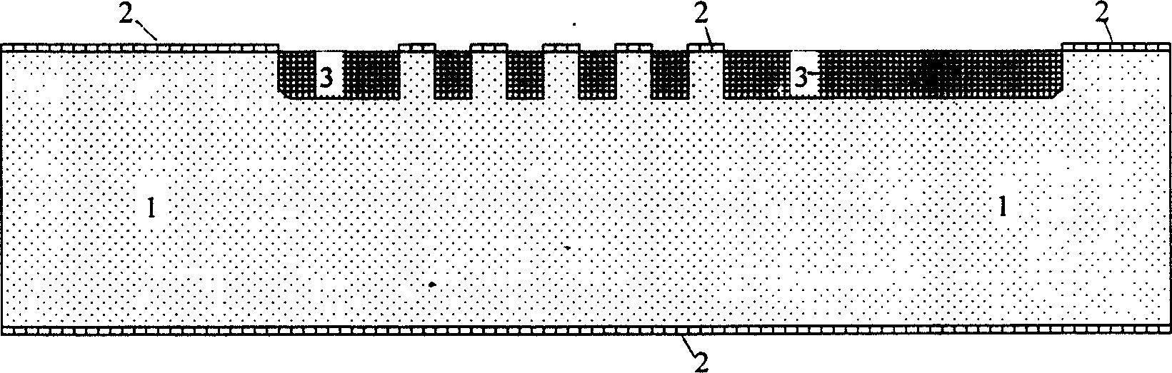
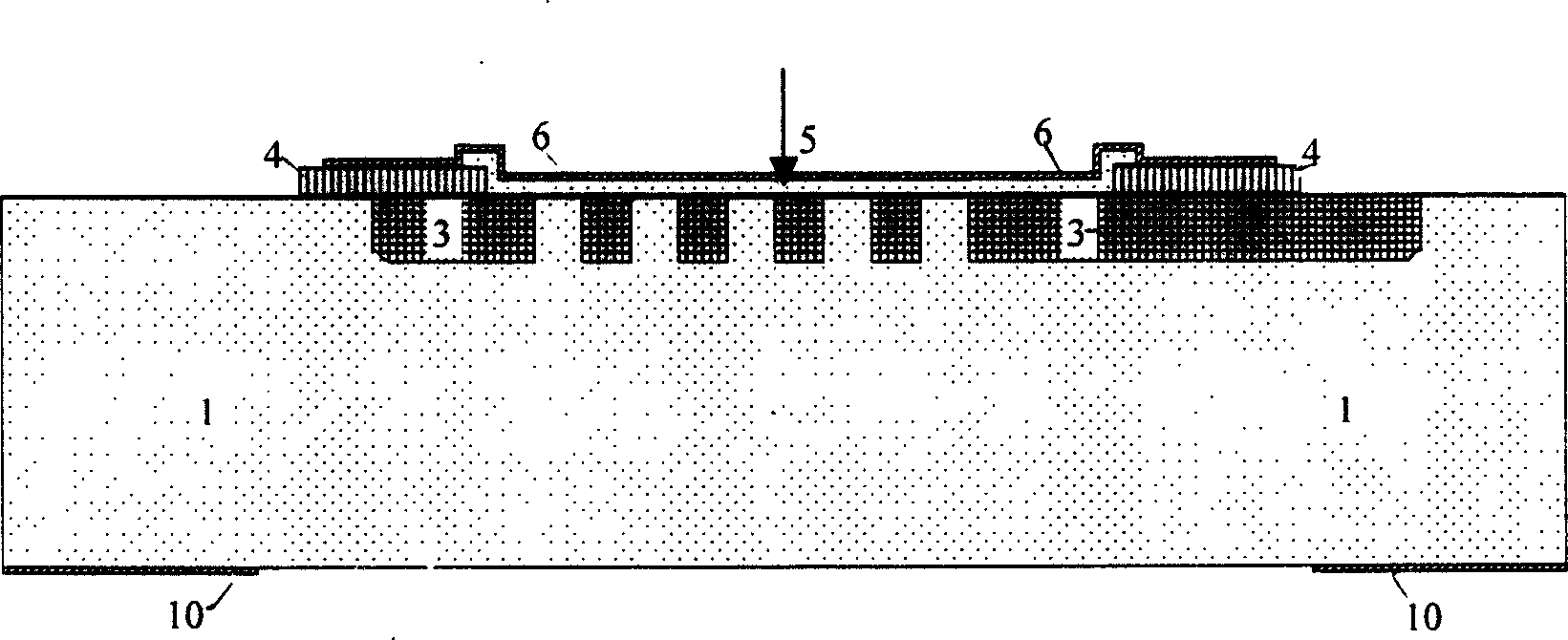
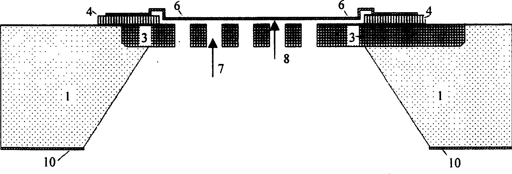
[0035] A kind of microphone chip provided by the present embodiment comprises an n-type silicon substrate 1, and boron is diffused on the front side of the silicon substrate 1 to form a p+ type doped layer 3 with a thickness of 3 or 20 microns; on the p+ type doped layer 3 deposited SiO 2 And photolithography, etch to form a ring-shaped isolation layer 4, the inner diameter of the annular isolation layer 4 is 500 or 3000 microns, and the radial width is 50 or 300 microns; a layer of silicon nitride is attached on the isolation layer 4. Circular vibrating membrane layer 6, deposition, photolithography, corrosion circular aluminum film and square electrode 9 on the vibrating membrane layer 6; as Figure 5 Shown; There is a layer of silicon nitride protection film 10 on the reverse side of the silicon substrate 1, a trapezoidal notch is etched out from the bottom surface of the silicon substrate 1, the depth of the trapezoidal notch reaches the p+ type doped layer 3, perpendicula...
Embodiment 2
[0037] Adopt preparation method of the present invention to prepare a microphone chip, its steps are as follows:
[0038] (1) n-type silicon wafer 1 undergoes a conventional high-temperature oxidation process to produce silicon dioxide 2 with a thickness of 0.5 microns. After photolithography, the high-temperature silicon dioxide is etched with hydrofluoric acid as a mask, and deep boron diffusion is performed on the front side of the silicon wafer. Form the p+ type doped layer 3 of the back plate, the depth is 5 microns, wherein the perforated part does not diffuse; as attached figure 1 shown.
[0039](2) Remove the high-temperature silicon dioxide mask with hydrofluoric acid; use plasma-enhanced chemical vapor deposition (PECVD) to deposit low-temperature silicon dioxide (LTO) on the front of the silicon wafer with a thickness of 0.5 microns, photolithography, hydrogen Fluoric acid corrodes the pattern of the annular isolation layer 4, the inner diameter of the annular ring...
Embodiment 3
[0044] (1) n-type silicon wafer 1 undergoes high-temperature oxidation to produce silicon dioxide with a thickness of 2 microns. After photolithography, use hydrofluoric acid to etch high-temperature silicon dioxide as a mask, and perform deep boron diffusion on the front of the silicon wafer to form a backplane The p+ type doped layer 3 has a depth of 15 microns, wherein the perforated part does not diffuse;
[0045] (2) Remove the high-temperature silicon dioxide mask with hydrofluoric acid; use plasma-enhanced chemical vapor deposition (PECVD) to deposit low-temperature silicon dioxide (LTO) on the front of the silicon wafer with a thickness of 6 microns, photolithography, hydrogen After hydrofluoric acid corrodes the annular isolation layer 4 pattern, the inner diameter of the annular ring is 3000 microns, and the width of the annular ring is 300 microns; Zinc oxide (ZnO) is deposited as a sacrificial layer by magnetron sputtering, with a thickness of 5 microns and a circul...
PUM
| Property | Measurement | Unit |
|---|---|---|
| thickness | aaaaa | aaaaa |
| width | aaaaa | aaaaa |
| thickness | aaaaa | aaaaa |
Abstract
Description
Claims
Application Information