Nano ceramic dopant, high-dielectric reduction-resistant multilayer ceramic capacitor dielectric material, and their preparation method
A capacitor dielectric and ceramic material technology, applied in the field of electronic materials, can solve the problems of high equipment requirements, long production cycle, complex process, etc., and achieve the effect of good performance repeatability, low cost and simple process
- Summary
- Abstract
- Description
- Claims
- Application Information
AI Technical Summary
Problems solved by technology
Method used
Image
Examples
preparation example Construction
[0054] (1) The preparation process and particle size control of the base material; U.S.Pat.5,319,517 uses the liquid phase method to synthesize BaTiO 3 , BaZrO 3 and CaTiO 3 Powder is used as the base material, and the present invention adopts submicron ultrafine (Ba, Ca) (Ti, Zr) O 3 as a base. In terms of particle size, both of them can reach submicron level, but there is BaTiO in U.S.Pat.5,319,517 3 , BaZrO 3 and CaTiO 3 The ratio of the three powders is mixed, and the production quality stability of the three powders must be controlled separately, so the risk of production process stability will inevitably increase.
[0055] (2) The preparation process and particle size control of the dopant, which is the most important difference. U.S. Pat. 5,319,517 prepares dopants by mixing solid substances such as oxides and carbonates, ball milling, and drying. Although it is emphasized that the average and maximum particle size of the dopant should be strictly controlled duri...
Embodiment 1
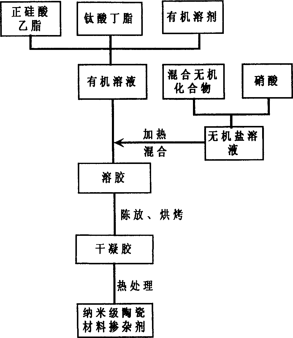
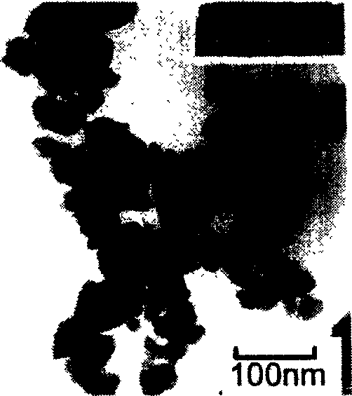
[0113] Embodiment 1: Process 1 is used to prepare nanoscale ceramic material dopant T1. Si:Y:Mn:Pr=1:4:2:2 (mole ratio) in sol-gel. Using process 1, ethyl tetrasilicate, acetylacetone and absolute ethanol are mixed into an organic solution, and the obtained gel is baked at 90°C for 3 days to obtain a dry gel, which is heat-treated at 800°C for 120 minutes Grind in an agate bowl. The particle size distribution of the obtained nano-dopants was observed with a transmission electron microscope (TEM). figure 2 A 100,000-fold TEM photograph of the nano-dopant T1 synthesized at 800°C is given.
Embodiment 2
[0114] Embodiment 2: Using process 2 to prepare an ultra-fine high dielectric resistance reduction multilayer ceramic capacitor dielectric material. The base material in the formula is (Ba 0.97 Ca 0.03 ) 1.001 (Ti 0.807 Zr 0.193 )O 3 . The base material accounts for 99.025%, 99.00% and 98.75% of the overall mass of the porcelain, and the nano-dopant T1 prepared in Example 1 of the present invention accounts for 0.75%, 1% and 1.25% of the overall mass in the sample respectively. The obtained ceramic material is ball-milled after adding appropriate organic additives, and then cast into a membrane, which is stacked with a printed Ni electrode to make a MLCC green embryo. After debinding in the air at 700°C, sinter in a reducing atmosphere at 1200°C for 2 hours (the heating rate and cooling rate are both 200°C / h, the atmosphere is changed from N 2 , H 2 and H 2 O control, oxygen partial pressure maintained at 10 -12 Pa), and then annealed under weak oxidation conditions ...
PUM
| Property | Measurement | Unit |
|---|---|---|
| particle size | aaaaa | aaaaa |
| particle size | aaaaa | aaaaa |
| particle size | aaaaa | aaaaa |
Abstract
Description
Claims
Application Information

