Plasma display device utilizing high-frequency preheating and plasma body discharging method
A plasma and high-frequency preheating technology, applied to static indicators, instruments, solid cathode components, etc., can solve problems such as weak vacuum ultraviolet light intensity, high manufacturing process requirements, and insufficient brightness of the display, and achieve increased density , improve the service life, good support effect
- Summary
- Abstract
- Description
- Claims
- Application Information
AI Technical Summary
Problems solved by technology
Method used
Image

Examples
Embodiment 1
[0023] Example 1: Plasma display using capacitive coupling for preheating
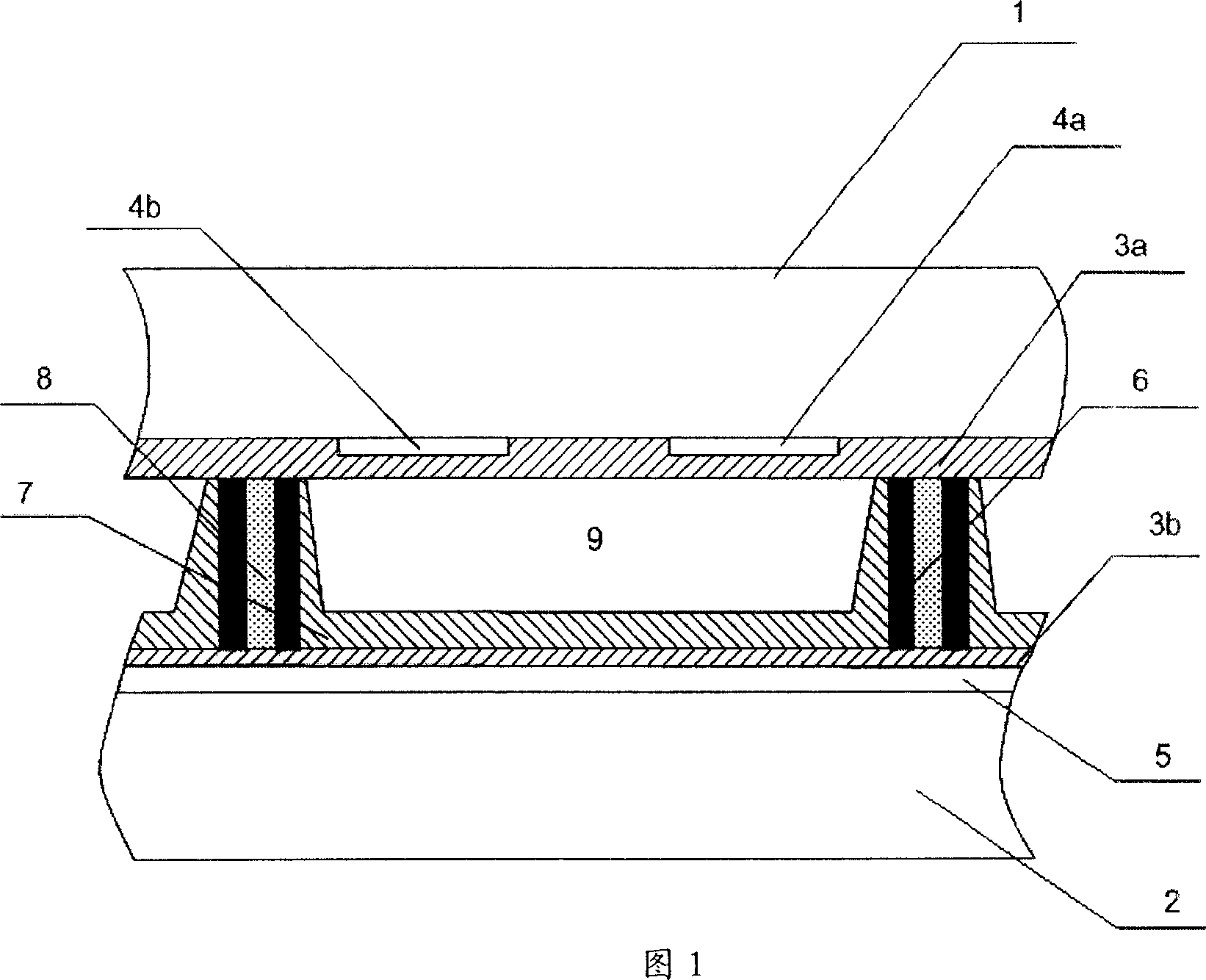
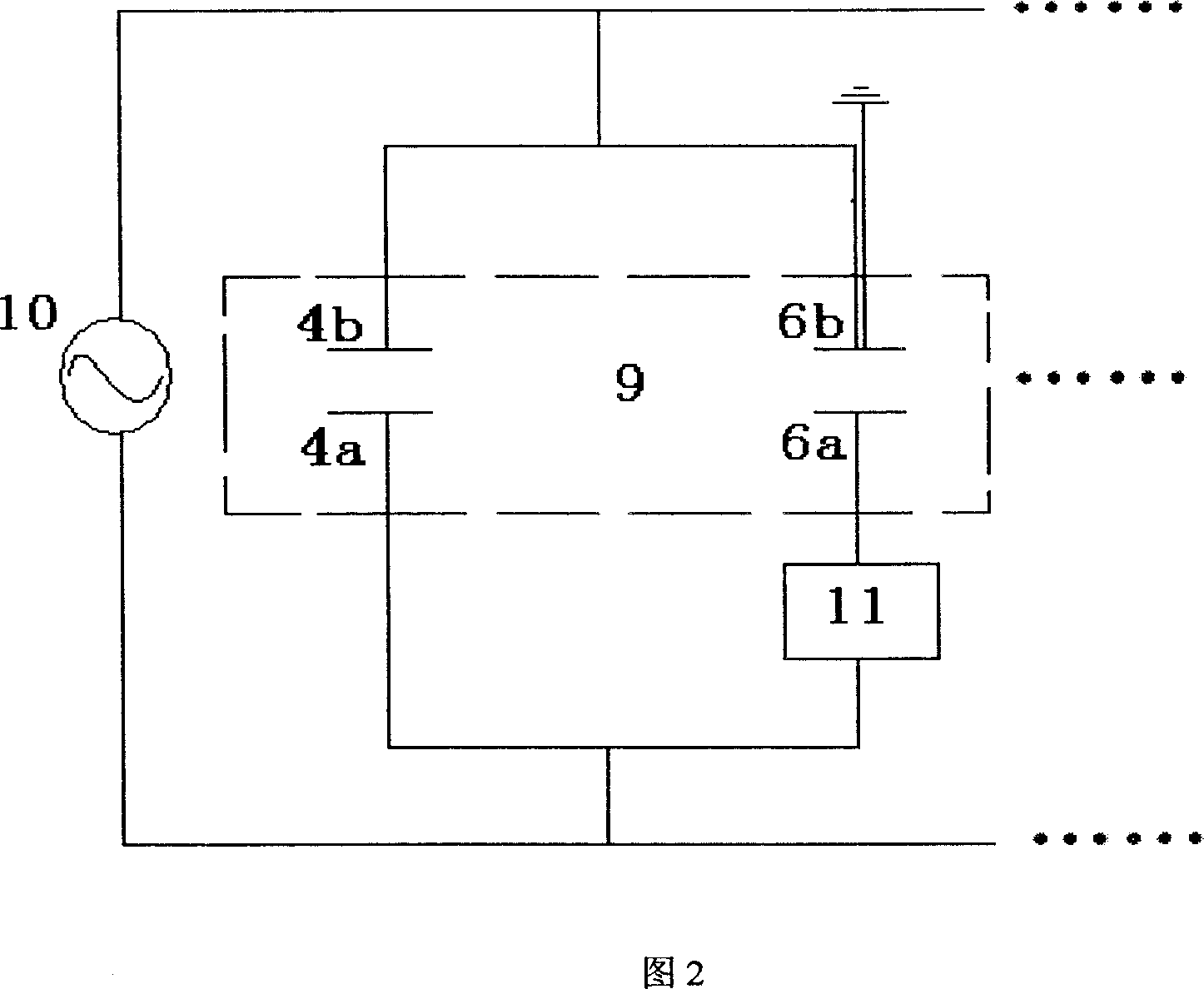
[0024] This embodiment is a typical three-electrode AC transmissive surface discharge plasma display. FIG. 1 shows a cross-sectional view of the discharge unit, and FIG. 2 is a schematic diagram of an equivalent circuit of a breakdown discharge and sustain discharge part of a discharge unit.
[0025] Referring to Figures 1 and 2: on the inner surface of the front substrate 1 made of high yield temperature glass, including glass of type PD200, there is a transparent film made of indium tin oxide (ITO) film with a thickness of 50 nanometers. Sustain electrodes 4a and 4b; a magnesium oxide dielectric layer 3a with a thickness of 20 micrometers is coated on the front substrate 1 and covers the surface of the sustain electrode 4; parallel to the front substrate 1, made of high yield temperature glass, including the model PD200 On the rear substrate 2 made of glass, facing towards the side of the sustain el...
Embodiment 2
[0031] Example 2: Plasma display using inductive coupling for preheating
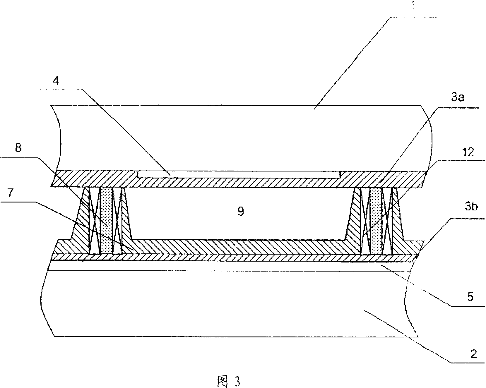
[0032] This embodiment is a typical DC transmission surface discharge plasma display. 3 is a cross-sectional view of a discharge unit of a DC discharge plasma display based on inductive coupling; FIG. 4 is an equivalent circuit diagram of a discharge unit of a DC discharge plasma display based on inductive coupling.
[0033] Referring to FIGS. 3 and 4 : on the inner surface of the front substrate 1 made of glass with a high yield temperature, including the glass of PD200, there is a transparent sustain electrode 4 made of a silver-tin film with a thickness of 5 microns; A 10-micron ruthenium oxide dielectric layer 3a is coated on the front substrate 1 and covers the surface of the sustain electrode 4; parallel to the front substrate 1, a rear substrate 2 made of high yield temperature glass including PD200 glass On the side facing the sustain electrode 4, there is an address electrode 5 made of nickel ...
PUM
| Property | Measurement | Unit |
|---|---|---|
| Thickness | aaaaa | aaaaa |
| Thickness | aaaaa | aaaaa |
| Thickness | aaaaa | aaaaa |
Abstract
Description
Claims
Application Information
 - R&D Engineer
- R&D Manager
- IP Professional
- Industry Leading Data Capabilities
- Powerful AI technology
- Patent DNA Extraction
Browse by: Latest US Patents, China's latest patents, Technical Efficacy Thesaurus, Application Domain, Technology Topic.
© 2024 PatSnap. All rights reserved.Legal|Privacy policy|Modern Slavery Act Transparency Statement|Sitemap