

Method and device with durable contact on silicon carbide
A technology of silicon carbide and silicon carbide layer, which is applied in the direction of semiconductor devices, semiconductor/solid-state device manufacturing, electrical components, etc., can solve the problems of easy degradation of Schottky contacts, achieve high current intensity, solve the problems of easy degradation, and improve performance Effect
- Summary
- Abstract
- Description
- Claims
- Application Information
AI Technical Summary
Problems solved by technology
Method used
Image

Examples
Embodiment 1
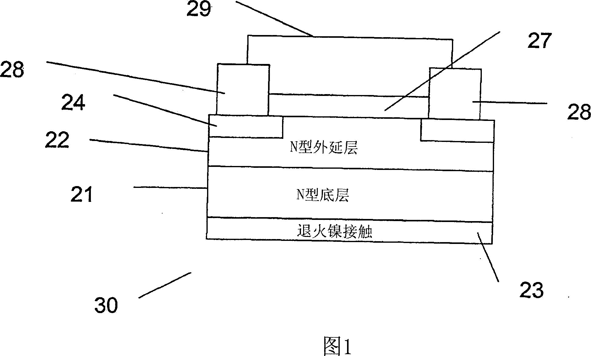
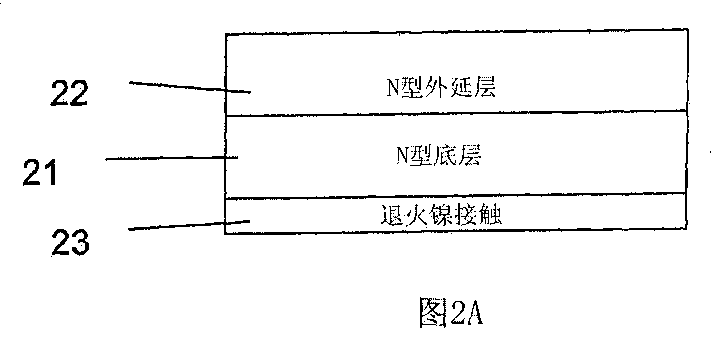
[0040] Termination-free Schottky diodes were fabricated on a 16 μm thick, 1.1E16cm -3 The N-type lightly doped silicon carbide epitaxial layer is carried out on the N-type heavily doped silicon carbide bottom layer EE15. On the heavily doped side of the bottom layer, an ohmic contact was made by depositing a layer of nickel to a thickness of 2500 Angstroms and vacuum annealing. On top of the epitaxial layer, a layer of rhenium with a thickness of 500 Angstroms was deposited by electron beam evaporation. The rhenium layer was patterned and etched, resulting in a 1.77E-4cm 2 positive pole. The volt-ampere characteristics of the final diode were measured by a Tektronix Model 577 waveform recorder. At a forward current of 0.7A, that is 4000A / cm 2 Under the current density, the diode still keeps working normally.
Embodiment 2
[0042] Termination-free Schottky diodes were fabricated on a 4.8 μm thick, 9.3E15 cm -3 The N-type lightly doped silicon carbide epitaxial layer is carried out on the N-type heavily doped silicon carbide bottom layer GB9. On the heavily doped side of the bottom layer, an ohmic contact was made by depositing a layer of nickel to a thickness of 2500 Angstroms and vacuum annealing. On the epitaxial layer, a 2500 Angstrom layer of rhenium was deposited by radio frequency magnetron sputtering. The rhenium layer was patterned and etched, yielding a 2.475E-4cm 2 positive pole. Finally the diode was reverse biased and the volt-ampere characteristics were measured.
[0043] Hatakayama (References 5, 6) argues that SiC Schottky diodes have reverse leakage current due to the tunneling effect at the metal-semiconductor junction which depends on the exponential relationship of electric field strength. Leakage current often limits the performance of the component before avalanche breakdow...
Embodiment 3
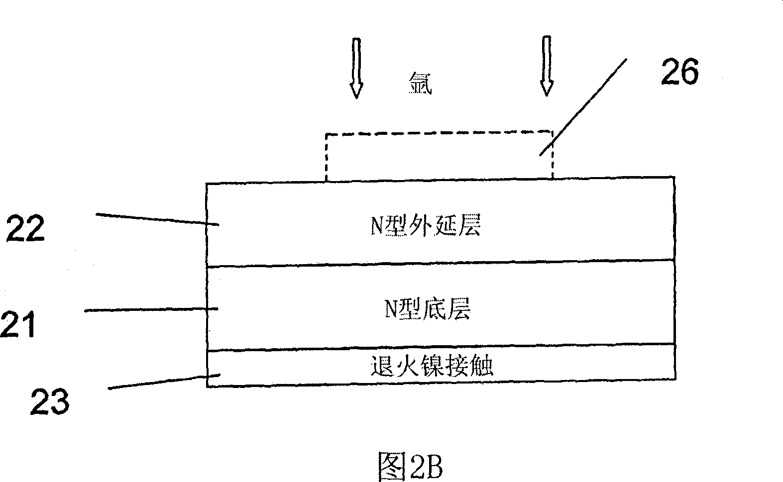
[0045] Schottky diodes with capped termination fields were fabricated on a 5 μm thick layer with a concentration of 1.1E16 cm -3 A three-layer N-type heavily doped SiC underlayer of a lightly doped SiC epitaxial layer is performed. On the heavily doped side of the bottom layer, an ohmic contact was made by depositing a layer of nickel to a thickness of 2500 Angstroms and vacuum annealing. The terminal field passes through with Ar + The beam is established by ion etching all surfaces of each wafer, the Ar + Ion beam energies vary, ranging from 250eV to 500eV. On the ion-etched surface of each wafer, a 2500 Angstrom layer of rhenium was deposited by radio frequency magnetron sputtering. The rhenium layer was patterned and etched, yielding a 4.9E-3cm 2 positive contact area. The volt-ampere (IV) characteristics of the final diode are then measured.
[0046] These diodes are rectifier diodes. The diode barrier heights measured from the voltammetry (IV) data are listed in Ta...
PUM
| Property | Measurement | Unit |
|---|---|---|
| thickness | aaaaa | aaaaa |
| thickness | aaaaa | aaaaa |
| thickness | aaaaa | aaaaa |
Abstract
Description
Claims
Application Information