Method and apparatus for surface preparation prior to epitaxial deposition

a surface preparation and epitaxial deposition technology, applied in the field of dielectric vessels, can solve the problems of reducing the thermal budget of wafers, reducing the radially outward velocity of gas, and reducing so as to increase the transport of volatile compounds and reduce the time needed for processing

Active Publication Date: 2020-01-28
AIXTRON AG
View PDF15 Cites 5 Cited by
  • Summary
  • Abstract
  • Description
  • Claims
  • Application Information

AI Technical Summary

Benefits of technology

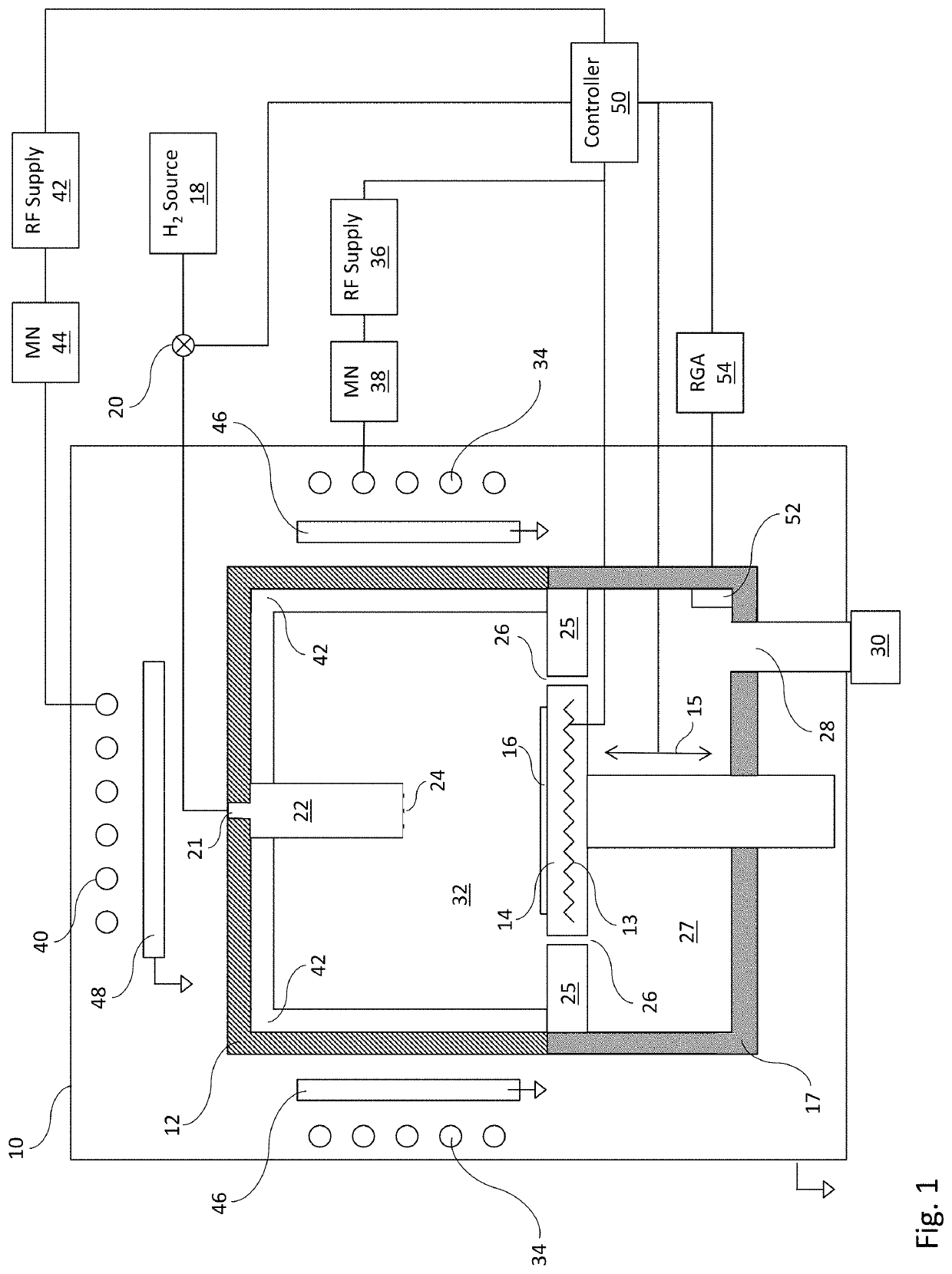
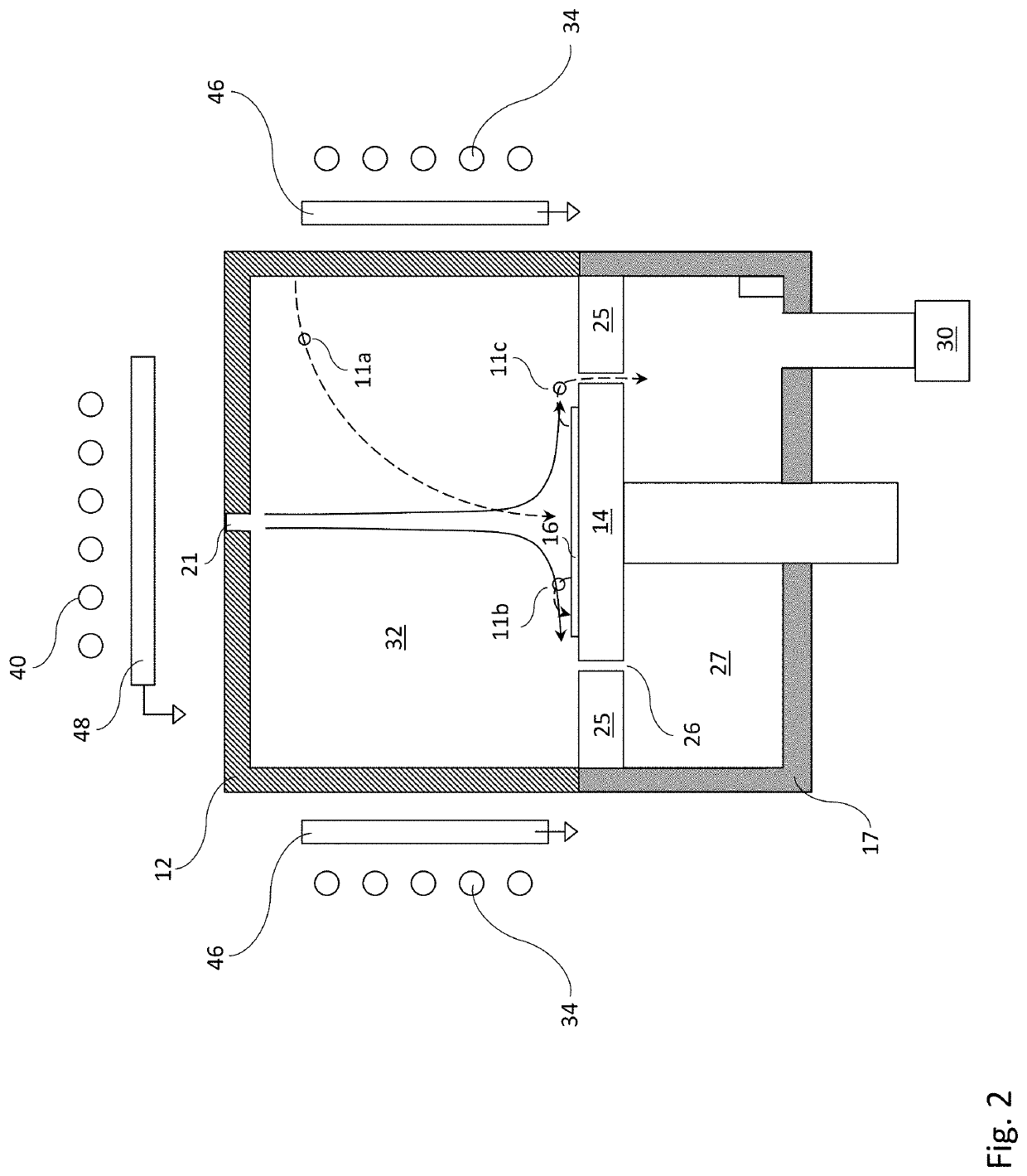
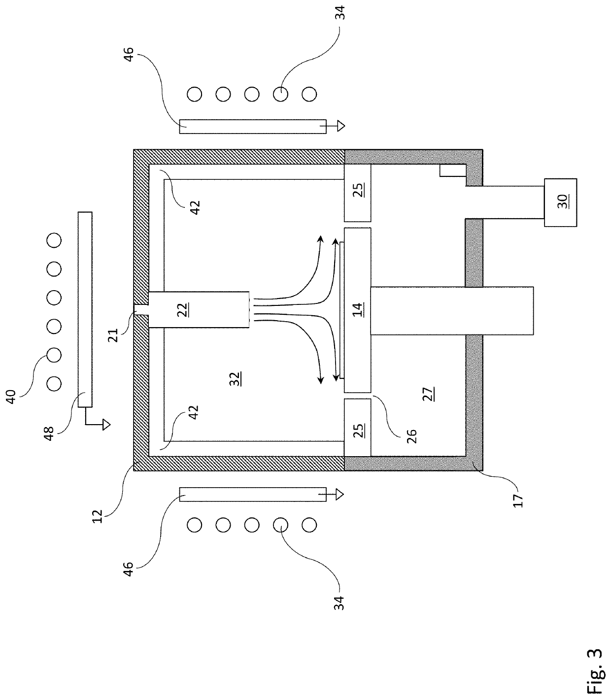
[0021]In accordance with some embodiments of the invention, hydrogen gas may be injected into the plasma volume via an injector nozzle which extends from the top of the dielectric vessel at least a third of a distance separating the top of the vessel from the surface of the semiconductor wafer. In an alternative embodiment, a mixture of hydrogen and a fluorinated gas such as nitrogen tri-fluoride may be injected. The injection of the hydrogen gas closer to the surface of the semiconductor wafer (generally less than about half the radius of the dielectric vessel) results in a higher radially outward velocity of the gas just above the surface of the wafer, as compared to when the injector is located more than half the chamber radius from the wafer surface. In embodiments where the gas is injected closer to the wafer rather than directly from a central gas inlet further from the wafer surface, the resulting effect is an increased transport of volatile compounds and other contaminants out of the dielectric vessel, and a reduction in the re-deposition of contaminants onto the surface of the semiconductor wafer. This elongated injector nozzle reduces the time needed for processing and in some cases improves the level of cleanliness of the wafer at the conclusion of the process.
[0022]In some embodiments of the invention, the dielectric vessel may have a short profile (e.g., height of dielectric vessel being less than or approximately equal to half of the radius of the dielectric vessel). The effect on the flow velocity field of the short profile is similar to the effect of the elongated injector nozzle, in that the gas just above the wafer surface may have a higher radial velocity (as compared to gas injected into a dielectric vessel with a tall profile).
[0023]In accordance with one embodiment of the invention, protective surface layers of materials that are inert to the reactive species from the plasma line the inner dielectric walls (i.e., the inner walls of the dielectric vessel). Such surface material layers may take the form of physical liners, or coatings thereupon, that may be disposed near inner surfaces of the dielectric vessel, or as coatings on the inner vessel wall. In some preferred embodiments, the protective surface or layers of material may be in the form of liners of thin sheet material made from crystalline silicon or polysilicon. Such liners may be about 1 mm or more in thickness and should be close to the dielectric walls, but do not need to be attached to the walls and may be free-standing. In other embodiments, the protective layers may consist of coatings on the inner wall of the dielectric vessel or coatings on separate non-conducting structures mounted inside the dielectric vessel near the walls, where such coatings may be of Y2O3 (densified yttria), La2Zr2O7 (lanthanum zirconate), titanium nitride, tantalum nitride or aluminum nitride, all of which are chemically very stable against reduction by atomic hydrogen. Such protective surface materials help prevent contaminants (which form as a result of reduction by atomic hydrogen) from being released from the dielectric vessel and diffusing through the gas to the surface of the semiconductor wafer.
[0024]In accordance with one embodiment of the invention, an exhaust restriction, formed by an exhaust restrictor, may prevent plasma from forming in the exhaust manifold and may further prevent volatile compounds and other chemical compounds containing contaminants from diffusing from the exhaust manifold back into the dielectric vessel. The exhaust restrictor is preferably made of a material such as silicon that will not introduce contaminants into the dielectric vessel, or may be made of dielectric materials that are coated with inert coatings such as the protective surfaces on or near the inner walls of the dielectric vessel.

Problems solved by technology

The inventors note that this process of Cohen produces a clean but damaged surface (due to argon ion bombardment) which is not suitable for the ensuing growth of a low-defect epitaxial film, and will also result in the removal of some of the substrate material.
However, this defect level is far too high as a method for surface preparation prior to hetero-epitaxy, particularly in ultra-sensitive areas of the transistor such as the channels.
However, such a high temperature may not be within the thermal budget for wafers once patterning for transistor fabrication has begun.
Chemical and mechanical effects on existing wafer patterns due to high temperature (>900° C.) with long bake time can cause problems in semiconductor devices such as: 1) loss of shallow implantation dopant of source / drain areas, 2) damage to patterned wafers with trenches for epitaxial growth; and 3) variations of critical device dimensions due to use of H2 bake in conjunction with HF clean.
), the amount of process time for thermal contaminant removal is excessive, because rates drop exponentially with temperature.
Such thermal / chemical cleans also may not remove surface contamination entirely, but usually yield an adequately crystalline surface upon which to grow succeeding epitaxial layers.
However, such cleaning processes usually leave unacceptable amounts of surface contaminants (>>1×10¹⁰ / cm2), caused by sputtering or release of contaminants from chamber walls, and almost always have ion bombardment of the wafer at energies sufficient to cause dislocations of atoms from the crystal lattice.
Such contaminant levels of oxygen will generally cause moderate to high defect densities in most epitaxy layers and other contaminants from the walls will worsen this situation.
Because of the above problems, no direct plasma clean has yet succeeded in meeting all requirements at advanced technology nodes (critical dimensions less than about 10 nm) for cleaning and surface preparation prior to more sensitive epitaxy processes of semiconducting films.
The defect level for a direct plasma clean in prior art technologies is too high, especially for hetero-epitaxy where a chemically different single-crystal layer is deposited upon the original material surface.
Such layers have a “lattice mismatch” between the crystals of the surface layer and substrate, which makes it especially sensitive to contaminants.
However, contaminants that may be sputtered or desorbed from the walls of the plasma chamber can be entrained with the activated gas flowing into the process chamber resulting in wafer contamination.
Further, such pre-clean processes typically are slow and usually fail to completely remove carbon and oxygen contaminants from the wafer unless there is an additional source of activation energy for surface reactions on the wafer.
However, it is very difficult to sustain a plasma, whether using RF or DC, where the plasma potential is so low that no ion damage or sputtering occurs.
UV radiation is one possible clean source of activation energy, but there has been no commercial technology utilizing it, and other data (U.S. Pat. No. 7,053,002) shows that it may require very high energy photons (e.g., VUV, such as from helium excitation) to give substantial etching or cleaning rates, which is difficult to provide from an external radiation source.
However, for patterned wafers this temperature is much too high and would cause damage to the pattern for transistors on the wafer, as is described above.
None of the prior art cleaning apparatus and methods, given the constraints of temperature and processing time, cleans a wafer surface and preserves surface crystallinity sufficiently well for epitaxial deposition of films of extremely low defect density.
Non-plasma methods such as Siebert ('077) require temperatures much greater than 1000° C. to have a process time less than hours, but patterned wafers cannot tolerate temperatures over 850° C. Other prior art methods and apparatus employing plasma to produce activated hydrogen species such as Hydrogen atoms have had deficiencies: causing crystalline damage to the critical surface layers of the wafer; permitting contaminants from the walls to get onto the wafer where they leave defects; removing too much of the wafer surface material; and leaving too many defects on the wafer surface to permit the growth of highest quality epitaxial films.

Method used


Image

  • Method and apparatus for surface preparation prior to epitaxial deposition
  • Method and apparatus for surface preparation prior to epitaxial deposition
  • Method and apparatus for surface preparation prior to epitaxial deposition

Examples


Embodiment Construction

[0044]In the following detailed description of the preferred embodiments, reference is made to the accompanying drawings that form a part hereof, and in which are shown by way of illustration specific embodiments in which the invention may be practiced. It should be understood that other embodiments may be utilized and structural changes may be made without departing from the scope of the present invention. Description associated with any one of the figures may be applied to a different figure containing like or similar components / steps. While the sequence diagrams each present a series of steps in a certain order, the order of some of the steps may be changed.

[0045]There are two, independent functions of the pre-treat wafer process for semiconductor IC fabrication that may be completed prior to epitaxy, and especially hetero-epitaxy. If not already apparent, the “treat” in “pre-treat” refers to the subsequent epitaxy treatment. The first function, wafer surface cleaning (also calle...


PUM

PropertyMeasurementUnit
temperatureaaaaaaaaaa
temperaturesaaaaaaaaaa

Abstract

During a pre-treat process, hydrogen plasma is used to remove contaminants (e.g., oxygen, carbon) from a surface of a wafer. The hydrogen plasma may be injected into the plasma chamber via an elongated injector nozzle. Using such elongated injector nozzle, a flow of hydrogen plasma with a significant radial velocity flows over the wafer surface, and transports volatile compounds and other contaminant away from the wafer surface to an exhaust manifold. A protective liner made from crystalline silicon or polysilicon may be disposed on an inner surface of the plasma chamber to prevent contaminants from being released from the surface of the plasma chamber. To further decrease the sources of contaminants, an exhaust restrictor made from silicon may be employed to prevent hydrogen plasma from flowing into the exhaust manifold and prevent volatile compounds and other contaminants from flowing from the exhaust manifold back into the plasma chamber.

Description

FIELD OF THE INVENTION[0001]The present invention relates to a dielectric vessel and its associated components, and a plasma-based and surface reconstruction process performed within the dielectric vessel for a surface preparation of wafers (unpatterned or patterned), prior to hetero- or homo-epitaxial deposition of a semiconducting material. Such epitaxy may be for either non-critical areas of a transistor or for critical areas such as the channels. The process utilizes hydrogen atoms produced in the plasma to etch native oxide and remove contaminants such as oxygen, carbon, and amorphous silicon without damaging the wafer surface so that the wafer has a high quality crystalline surface (composed of silicon or III-V layers), ready for a high-quality epitaxy of III-V or other semiconducting materials.BACKGROUND[0002]U.S. Pat. No. 8,152,918 to Zhang et al. describes a pre-epitaxial deposition cleaning process in which an unspecified type of radio frequency (RF) excited plasma is form...

Claims


Application Information

Patent Timeline
Patent Type & Authority Patents(United States)
IPC IPC(8): C30B25/08H01L21/687H01L21/02C30B25/18H01L21/3065H01J37/32H01L21/67
CPCH01J37/32522H01J37/32504H01J37/32495H01L21/02002H01L21/02315C30B25/186H01L21/02043H01L21/68707C30B25/08H01L21/3065H01L21/67051H01L2924/3011H01L21/02661H01J37/321H01J37/3244H01J37/32477H01J37/32651H01J37/32834H01L21/02046H01J2237/335H01L21/02381H01L21/02538
Inventor SAVAS, STEPHEN EDWARDSALDANA, MIGUEL ANGELCOSSENTINE, DAN LESTERKIM, HAE YOUNGTAMILMANI, SUBRAMANIANMUKHERJEE, NILOYKARIM, M ZIAUL
Owner AIXTRON AG
Why Eureka
Try Eureka