Computationally efficient X-ray based overlay measurement

a computation-efficient, overlay measurement technology, applied in the direction of material analysis using wave/particle radiation, instruments, photomechanical equipment, etc., can solve the problems of increasing measurement applications, characterization becoming more difficult, and the approach cannot reliably overcome the fundamental challenges of many advanced targets, so as to maximize the precision and accuracy of overlay measurements, the effect of increasing the independence of overlay signals

Active Publication Date: 2020-01-28
KLA CORP
View PDF59 Cites 1 Cited by
  • Summary
  • Abstract
  • Description
  • Claims
  • Application Information

AI Technical Summary

Benefits of technology

[0024]In a further aspect, the estimation of overlay involves a parameterization of the intensity modulations of common orders such that a low frequency shape modulation is described by a set, or ratio, of basis functions and a high frequency overlay modulation is described by an affine-circular function that includes a parameter indicative of the overlay. By fitting measured intensity signals to phenomenological, simple functions, overlay offsets associated with multiple layers may be estimated in a computationally efficient manner. As a result, the measurements are performed at a relatively low computational cost and without external reference metrology, thus overcoming the limitations of current methods based on SEM, optical metrology, or other proposed x-ray metrology techniques.
[0025]In another aspect, a set of angles of incidence and azimuth angles are designed to enhance the spatial frequency of the overlay modulation such that sensitivity to overlay is increased and correlation between overlay and shape parameters is minimized.
[0027]In another aspect, the overlay metrology target is optimized specifically to increase the independence of overlay signals from each the constituent layers and maximize the precision and accuracy of the overlay measurements.

Problems solved by technology

However, these approaches have not reliably overcome fundamental challenges associated with measurement of many advanced targets (e.g., complex 3D structures, structures smaller than 10 nm, structures employing opaque materials) and measurement applications (e.g., line edge roughness and line width roughness measurements).
As devices (e.g., logic and memory devices) move toward smaller nanometer-scale dimensions, characterization becomes more difficult.
Devices incorporating complex three-dimensional geometry and materials with diverse physical properties contribute to characterization difficulty.
For example, modern memory structures are often high-aspect ratio, three-dimensional structures that make it difficult for optical radiation to penetrate to the bottom layers.
Optical metrology tools utilizing infrared to visible light can penetrate many layers of translucent materials, but longer wavelengths that provide good depth of penetration do not provide sufficient sensitivity to small anomalies.
As a result, the parameters characterizing the target often cannot be reliably decoupled with available measurements.
For some structural parameters, such as edge placement error (EPE), there is currently no high throughput (e.g., optical) measurement solution.
Optical radiation is often unable to penetrate layers constructed of these materials.
As a result, measurements with thin-film scatterometry tools such as ellipsometers or reflectometers are becoming increasingly challenging.
Unfortunately, these specialized target structures often do not conform to the design rules of the particular semiconductor manufacturing process being employed to generate the electronic device.
This leads to errors in estimation of overlay errors associated with actual device structures that are manufactured in accordance with the applicable design rules.
In one example, image-based optical overlay metrology is severely limited by the resolution of imaging at optical wavelengths.
Moreover, the accuracy of this measurement approach degrades dramatically in the presence of any asymmetry in any of the layers where overlay is measured.
In addition, this approach cannot differentiate between positive and negative overlay errors in a single measurement.
In addition, the accuracy of this approach degrades dramatically in the presence of any asymmetry in any of the layers where overlay is measured.
Atomic force microscopes (AFM) and scanning-tunneling microscopes (STM) are able to achieve atomic resolution, but they can only probe the surface of the specimen.
In addition, AFM and STM microscopes require long scanning times.
Scanning electron microscopes (SEM) achieve intermediate resolution levels, but are unable to penetrate structures to sufficient depth without destroying the sample.
Thus, high-aspect ratio holes are not characterized well.
In addition, the required charging of the specimen has an adverse effect on imaging performance.
Transmission electron microscopes (TEM) achieve high resolution levels and are able to probe arbitrary depths, but TEM requires destructive sectioning of the specimen.
Thus, either an external metrology system or a computationally expensive simulation is required to calibrate out the effect of CD.
Either of these approaches is limited in accuracy and precision due to the high correlation between CD parameters (e.g., asymmetry) and overlay.
Currently there is no high-throughput, optical metrology solution for EPE measurements and many on-device overlay measurement applications.
In addition, the absence of adequate metrology makes it challenging to define control schemes to improve device yield.
Future metrology applications present challenges for metrology due to increasingly small resolution requirements, multi-parameter correlation, increasingly complex geometric structures, and increasing use of opaque materials.
In some embodiments, a multiple layer overlay metrology target is designed with different pitch orientations at different layers such that a diffraction order arising from one layer constructively interferes with a different diffraction order of another layer.

Method used


Image

  • Computationally efficient X-ray based overlay measurement
  • Computationally efficient X-ray based overlay measurement
  • Computationally efficient X-ray based overlay measurement

Examples


Embodiment Construction

[0045]Reference will now be made in detail to background examples and some embodiments of the invention, examples of which are illustrated in the accompanying drawings.

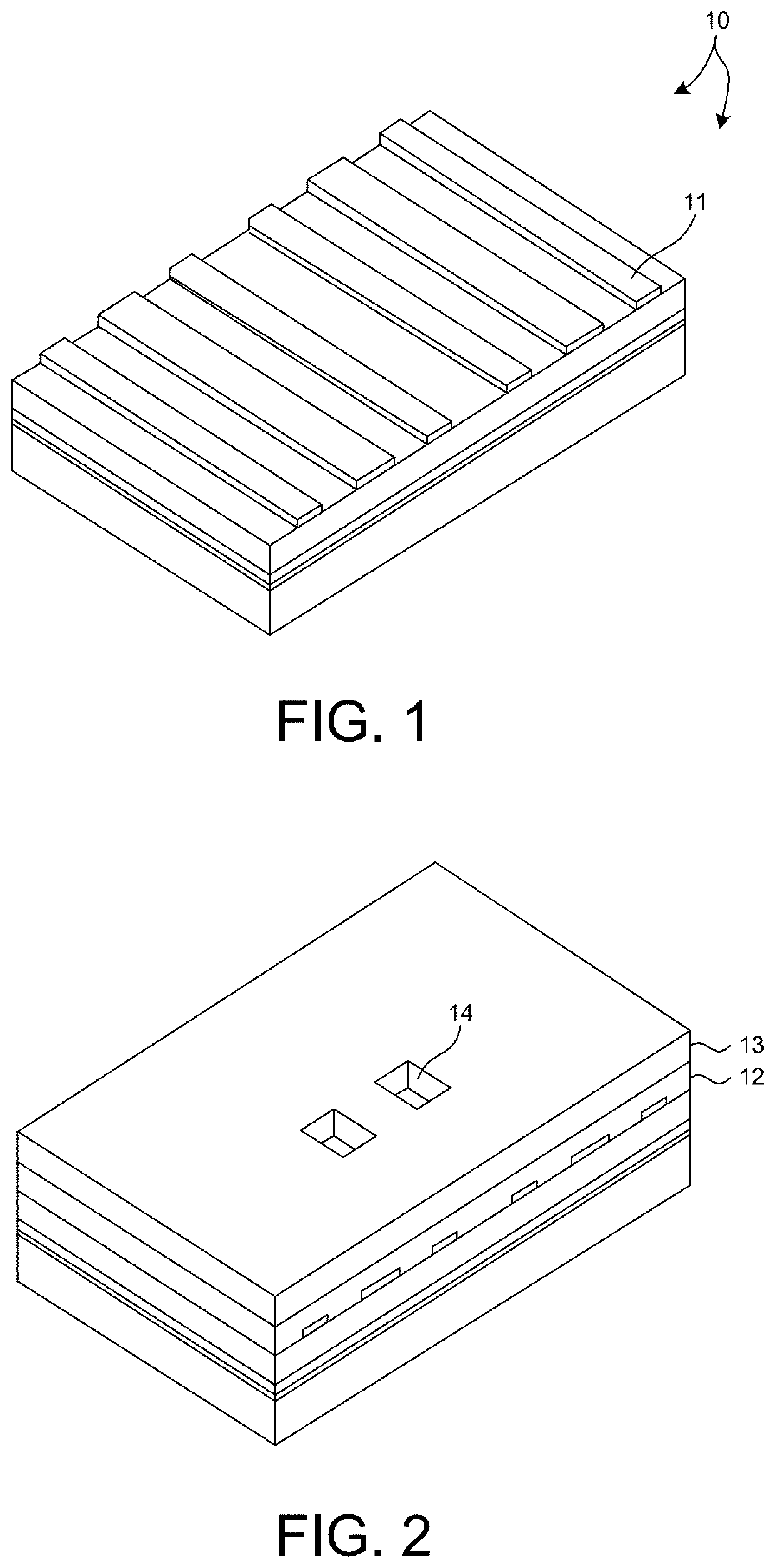
[0046]FIG. 1 depicts a hardmask pattern of line structures 11 fabricated in a static random access memory (SRAM) area 10 of a microelectronic chip. The complex layout of the active region is created by combining multiple patterning techniques with cut masks. Cut masks selectively remove portions of the hardmask layer that is used to pattern the substrate into active regions. FIG. 2 depicts a bottom anti-reflective coating (BARC) layer 12 and a resist layer 13 disposed on top of the pattern of line structures depicted in FIG. 1. The resist layer is used to selectively remove part of the hardmask pattern below the openings 14 of the resist layer 13. As depicted in FIG. 1, the hardmask pattern of line structures 11 is buried by the BARC layer 12, even within the openings 14 of the resist layer 13.

[0047]To provide adequat...


PUM

PropertyMeasurementUnit
roughnessaaaaaaaaaa
thicknessesaaaaaaaaaa
sizeaaaaaaaaaa

Abstract

Methods and systems for performing overlay and edge placement errors of device structures based on x-ray diffraction measurement data are presented. Overlay error between different layers of a metrology target is estimated based on the intensity variation within each x-ray diffraction order measured at multiple, different angles of incidence and azimuth angles. The estimation of overlay involves a parameterization of the intensity modulations of common orders such that a low frequency shape modulation is described by a set of basis functions and a high frequency overlay modulation is described by an affine-circular function including a parameter indicative of overlay. In addition to overlay, a shape parameter of the metrology target is estimated based on a fitting analysis of a measurement model to the intensities of the measured diffraction orders. In some examples, the estimation of overlay and the estimation of one or more shape parameter values are performed simultaneously.

Description

CROSS REFERENCE TO RELATED APPLICATION[0001]The present application for patent claims priority under 35 U.S.C. § 119 from U.S. provisional patent application Ser. No. 62 / 154,108, entitled “Model-Free Method and Apparatus for Measuring Semiconductor Device Overlay Using X-ray Metrology Techniques,” filed Apr. 28, 2015, the subject matter of which is incorporated herein by reference in its entirety.TECHNICAL FIELD[0002]The described embodiments relate to metrology systems and methods, and more particularly to methods and systems for improved measurement accuracy.BACKGROUND INFORMATION[0003]Semiconductor devices such as logic and memory devices are typically fabricated by a sequence of processing steps applied to a specimen. The various features and multiple structural levels of the semiconductor devices are formed by these processing steps. For example, lithography among others is one semiconductor fabrication process that involves generating a pattern on a semiconductor wafer. Additi...

Claims


Application Information

Patent Timeline
Patent Type & Authority Patents(United States)
IPC IPC(8): G01N23/207
CPCG01N23/207G01N2223/611G01N23/20008G01N23/201G03F7/0035G03F7/70633G21K1/062
Inventor HENCH, JOHNSHCHEGROV, ANDREI V.BAKEMAN, MICHAEL S.
Owner KLA CORP
Why Eureka
Try Eureka