
Transparent flexible silver nanowire-based conducting film and manufacturing method thereof

Active Publication Date: 2020-08-04
KOREA INST OF SCI & TECH
View PDF19 Cites 2 Cited by
  • Summary
  • Abstract
  • Description
  • Claims
  • Application Information

AI Technical Summary

Benefits of technology

The present invention provides a transparent flexible silver nanowire-based conducting film that can be mass-produced and large-area producible with excellent electrical conductivity, light transmittance, and electromagnetic interference shielding performance. The method involves coating conductive nanowires on a flexible substrate, sintering them using a wet sintering process, and coating a polymer layer in which graphene flakes are dispersed on the flexible substrate with the conductive nanowires. The flexible substrate can be dried for 0.1 to 3 hours at a temperature range from 50° C to 130° C. The flexible substrate can be dried for 0.5 to 1.5 hours at a temperature range from 105° C to 115° C. The flexible substrate can be dried for 1 to 12 hours at a temperature range from 20° C to 100° C. The polymer layer can include polyurethane. The transparent flexible silver nanowire-based film can be used for electrodes and electromagnetic interference shielding. The flexible substrate can be selected from a group consisting of PET, PC, PMMA, TAC, PEN, and PES. The conductive nanowires can include metal, conductive ceramics, conductive polymers, and composites thereof.

Problems solved by technology

However, as flexible devices become miniaturized and more flexible, interference occurs due to electromagnetic waves generated by each independent system, which may cause a problem in operating the device or a shortened lifespan.
In addition, research has shown that electromagnetic waves generated inside of a device may directly cause harmful influence on a human body.
Transparent conducting films used in flexible display devices are required to simultaneously have high electrical conductivity, high shielding property, light transmissivity, and high flexibility, but a shielding material that satisfies all of these properties has not yet been developed.
However, in the case of flexible transparent shielding material, it is important to increase electric conductivity without reducing transmittance in order to enhance shielding performance because there is a limitation on the thickness of the shielding material due to required high light transmissivity.
However, by the nature of the oxide conductor, ITO easily cracks under a threshold radius of curvature condition (>7 mm), and hence it is not suitable as a flexible transparent electrode and / or electromagnetic interference shielding material.
Thus, Al-doped ZnO has a limited shielding property and hence has a limitation as a flexible transparent electromagnetic interference shielding material.
Metal mesh exhibits a high electrical conductivity and a high electromagnetic interference shielding efficiency along with high transmittance, but the process thereof is completed and requires high cost and there is an issue of vulnerability to a repetitive fatigue characteristic.
Multi-layer graphene produced to enhance the shielding performance shows a high shielding performance of 19.14 dB (18-26.5 GHz) at a transmittance of 80.5%, but the process thereof is very complicated and large-area production is difficult.
Despite these advantages, the Ag NWs have weakened networking properties due to an insulating capper used to anisotropically grow the nanowires during a polyol synthesis process.
Due to this fact, bonding is not properly performed at junctions between the nanowires so that contact resistance is increased.
Also, the Ag NWs has a weak bonding strength to a substrate and is vulnerable to moisture and oxygen because it is made of metal.
These characteristics are problems that must be solved when the Ag NWs are applied to electronic devices.
However, there are drawbacks of a lack of scalability to mass-production and large-area processes and requirement of long process time and high cost.

Method used


Image

  • Transparent flexible silver nanowire-based conducting film and manufacturing method thereof
  • Transparent flexible silver nanowire-based conducting film and manufacturing method thereof
  • Transparent flexible silver nanowire-based conducting film and manufacturing method thereof

Examples


Embodiment Construction

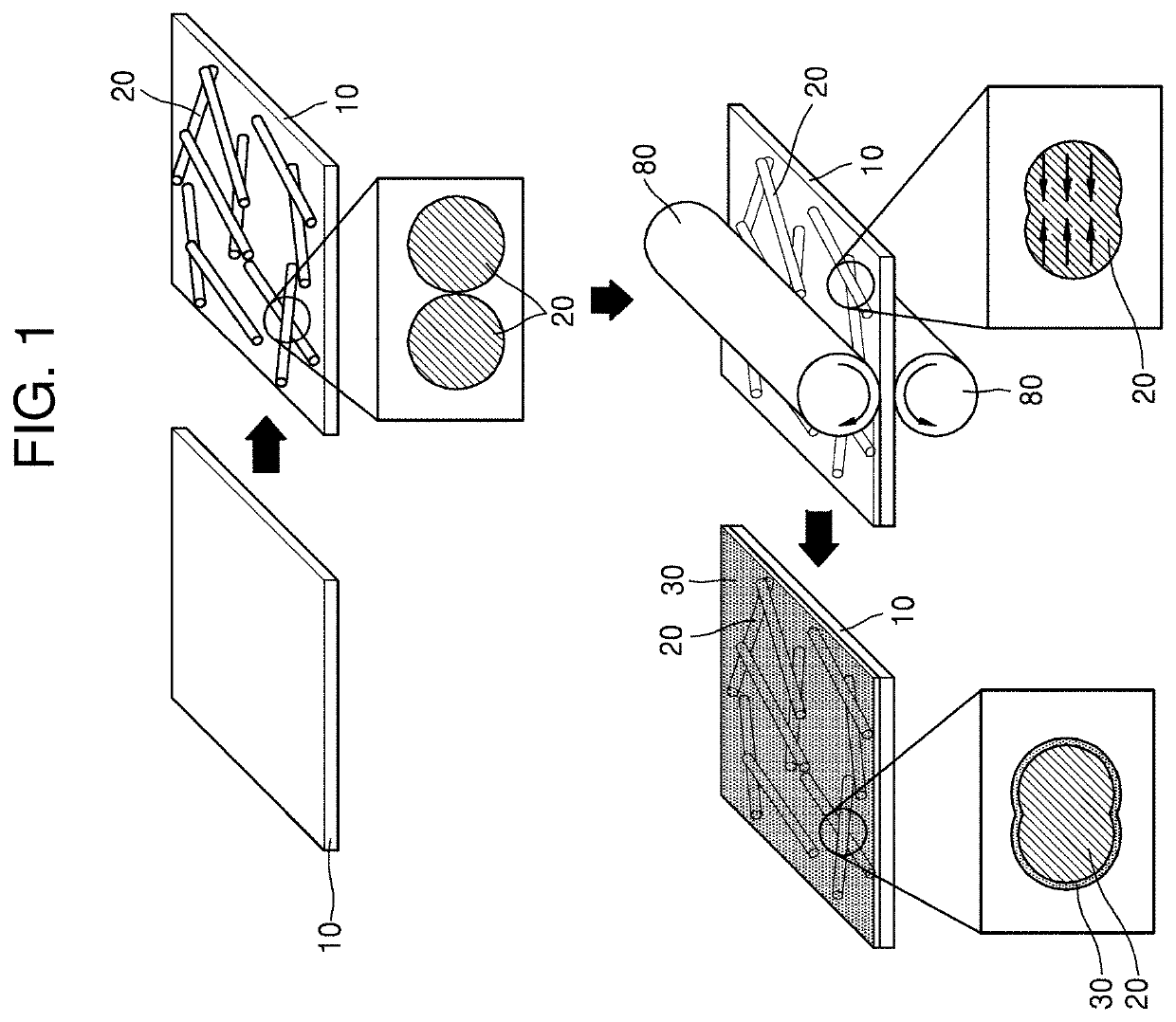
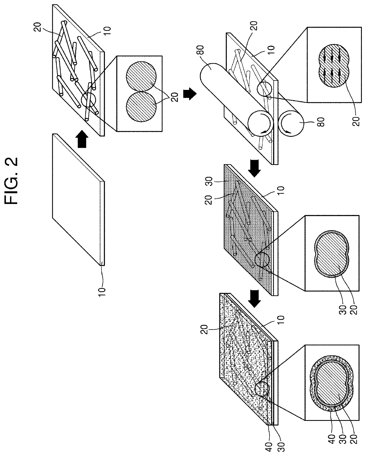
[0044]Hereinafter, the present invention will be described in detail by explaining embodiments of the invention with reference to the attached drawings. The invention may, however, be embodied in many different forms and should not be construed as being limited to the embodiments set forth herein; rather, these embodiments are provided so that this disclosure will be thorough and complete, and will fully convey the concept of the invention to one of ordinary skill in the art. In the drawings, the sizes of elements may be exaggerated or reduced for convenience of explanation.

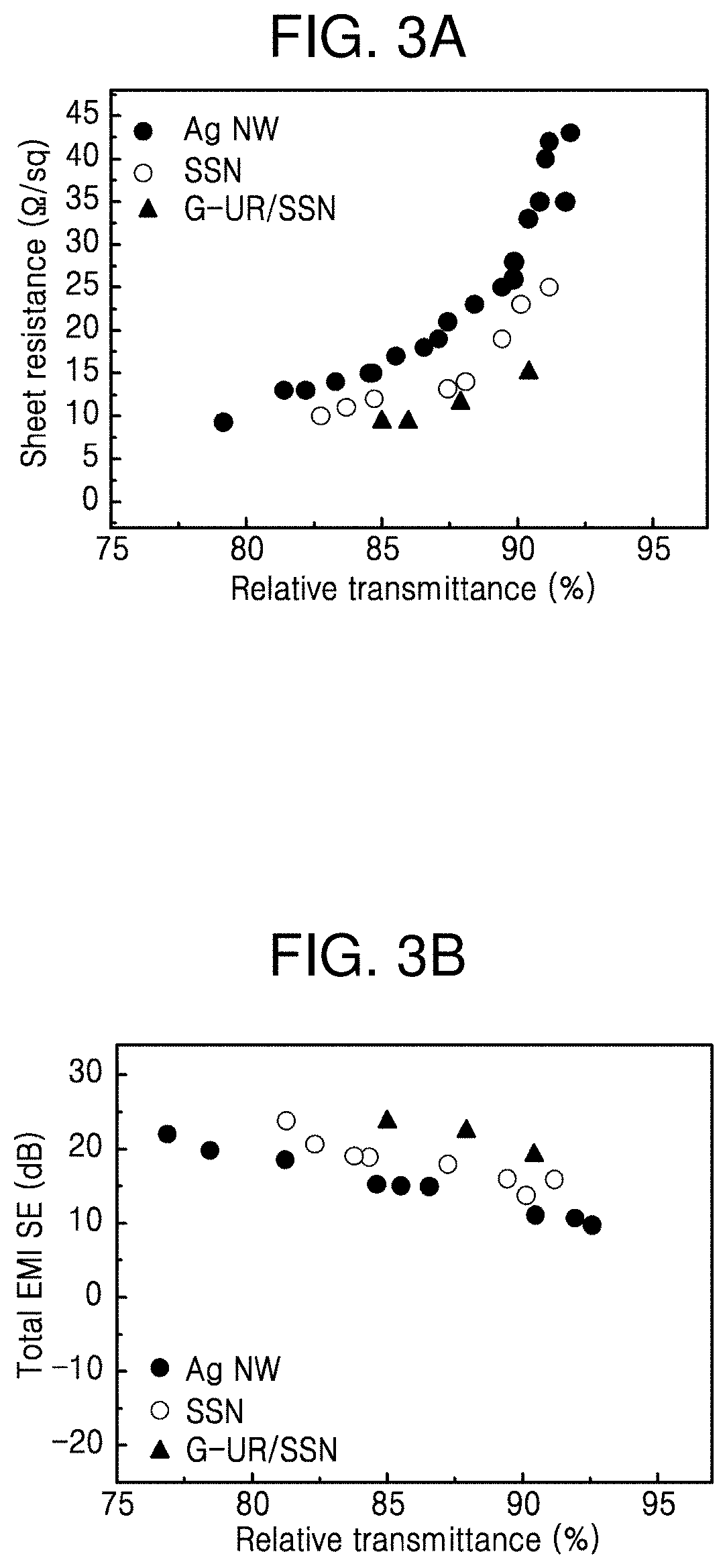
[0045]In recent years, rapidly increasing demands for highly flexible devices have increased the need for a flexible transparent conducting film against the electromagnetic interference that can cause these devices to malfunction and that poses a hazard to human health. Furthermore, because highly flexible devices are prone to repetitive fatigue, due to repeated bending or stretching, and / or corrosion and contami...


PUM

PropertyMeasurementUnit
Temperatureaaaaaaaaaa

Abstract

A method of manufacturing a transparent flexible silver nanowire-based conducting film and a transparent flexible silver nanowire-based conducting film are provided. The method includes coating conductive nanowires, which shield and absorb electromagnetic interference, on a flexible substrate, sintering the conductive nanowires using a wet sintering process, and coating a polymer layer in which graphene flakes are dispersed on the flexible substrate with the conductive nanowires formed thereon.

Description

CROSS-REFERENCE TO RELATED APPLICATION(S)[0001]This application claims the benefit under 35 USC § 119(a) of Korean Patent Application No. 10-2019-0031868, filed on Mar. 20, 2019, in the Korean Intellectual Property Office, the entire disclosure of which is incorporated herein by reference for all purposes.BACKGROUND1. Field[0002]The following description relates to a transparent flexible silver nanowire-based conducting film and manufacturing method thereof, and more specifically, to a transparent flexible silver nanowire-based conducting film for electrodes and / or electromagnetic interference shielding applicable to flexible devices and a manufacturing method thereof.2. Description of Related Art[0003]Recently, there is a growing demand for flexible devices in a variety of designs with portability and no restrictions in shape and form, such as wearable devices and foldable displays. However, as flexible devices become miniaturized and more flexible, interference occurs due to elect...

Claims


Application Information

Patent Timeline
IPC IPC(8): H05K9/00B32B15/02B32B37/04
CPCH05K9/0094H05K9/0086H05K9/0088B32B15/02B32B2307/212H05K9/0081H05K9/0096H01B1/24H01B5/14H05K9/0083
Inventor KIM, SANG WOOCHOI, JONG HAN
Owner KOREA INST OF SCI & TECH
Learn More