Surface mount packaging for single mode electro-optical module

a technology of electro-optical modules and surface mounts, applied in the direction of optical elements, electromagnetic transceivers, instruments, etc., can solve the problems of unreliable power consumption figures of pluggable modules, system implementations that have not yet changed significantly, and the center is becoming not only faster, but often larger

Active Publication Date: 2021-08-17
ELECTROPHOTONIC IC INC
View PDF15 Cites 0 Cited by
  • Summary
  • Abstract
  • Description
  • Claims
  • Application Information

AI Technical Summary

Benefits of technology

[0024]Electro-optical modules of embodiments described herein enable optical ports to be implemented with higher density, and potentially with densities comparable to, or greater than, densities of copper links on the PCB faceplates. This packaging configuration also enables distribution of the Electro-Optical (E / O) modules on the PCB close to, i.e. in physical proximity to, the internal switching chips on the PCB, in a manner analogous to the copper links of earlier times. When the E / O module is mounted adjacent to the core switch chip that it is communicating with, the communication link is much shorter and easier to implement in a way that the signal is clean and error free, and consumes less power. By distributing the optical modules over the board, they can be more effectively cooled by spreading the heat dissipation across the entire area of the board and picking up airflow across the PCB.
[0025]Moreover, implementing the electro-optical modules in a package form factor that is similar to conventional surface mountable ball grid array packages allows them to be shipped in tape and reel format, so that the printed circuit board can be assembled in the same way as if there were only electronics on the board, e.g. using surface mount, pick-and-place machines, followed by solder reflow ovens. The optical packages are configured to withstand the heat of the reflow ovens, so that expensive high-speed electrical sockets are not required for the optical modules, because direct surface mount soldering is possible and standard re-work methods and tools can be used to rework defects on the board including the optical modules. This approach also improves signal integrity of the links on the PCB, e.g. to enable 25G or higher speed links. Since surface mounting of the CBGA package is accomplished with the optical fiber connectors detached, the optical fiber connectors can be fabricated from materials and components that do not need to be able to withstand high temperature PCB processing, such as solder reflow.

Problems solved by technology

Unfortunately, the 10G copper standard took several years to achieve the required performance and power consumption specifications, and even then, was only able to achieve a limited reach of about 50 meters, at a time when data centers were becoming not only faster, but often larger.
Although the roles of copper and fiber interconnect are reversing, system implementations have not yet changed significantly.
However, there are a number of challenges with existing pluggable modules.
This presents a challenge with respect to power consumption figures for pluggable modules, particularly as the demand for speed continues to increase.
Also, the speeds of optical links grow to 25 Gb / s and 56 Gb / s per lane, the design of connections between the core switching chips on the board and the pluggable optical modules on the faceplate becomes electrically more challenging, due to the interconnect lengths and speeds.

Method used


Image

  • Surface mount packaging for single mode electro-optical module
  • Surface mount packaging for single mode electro-optical module
  • Surface mount packaging for single mode electro-optical module

Examples


first embodiment

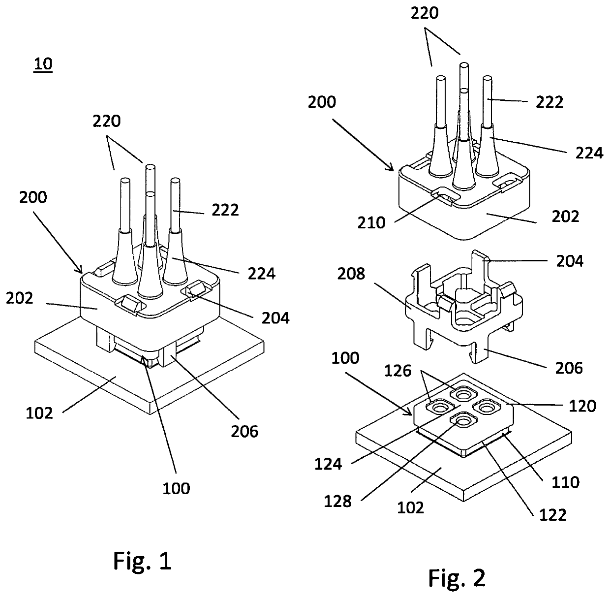
[0080]An isometric schematic view of an assembly 10 comprising an electro-optical module 100 of the invention, surface mounted on a substrate comprising a printed circuit board (PCB) 102, is shown in FIG. 1. An optical connector 200 having a connector body 202 carrying a plurality of four single mode optical fiber pigtails 220, with strain relief boots 224, is shown plugged into the electro-optical module 100. Latch means comprising latch elements 204 and 206 secure the optical fiber connector 200 to the electro-optical module 100.

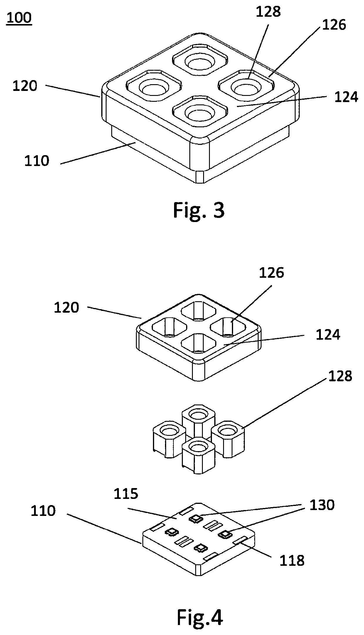
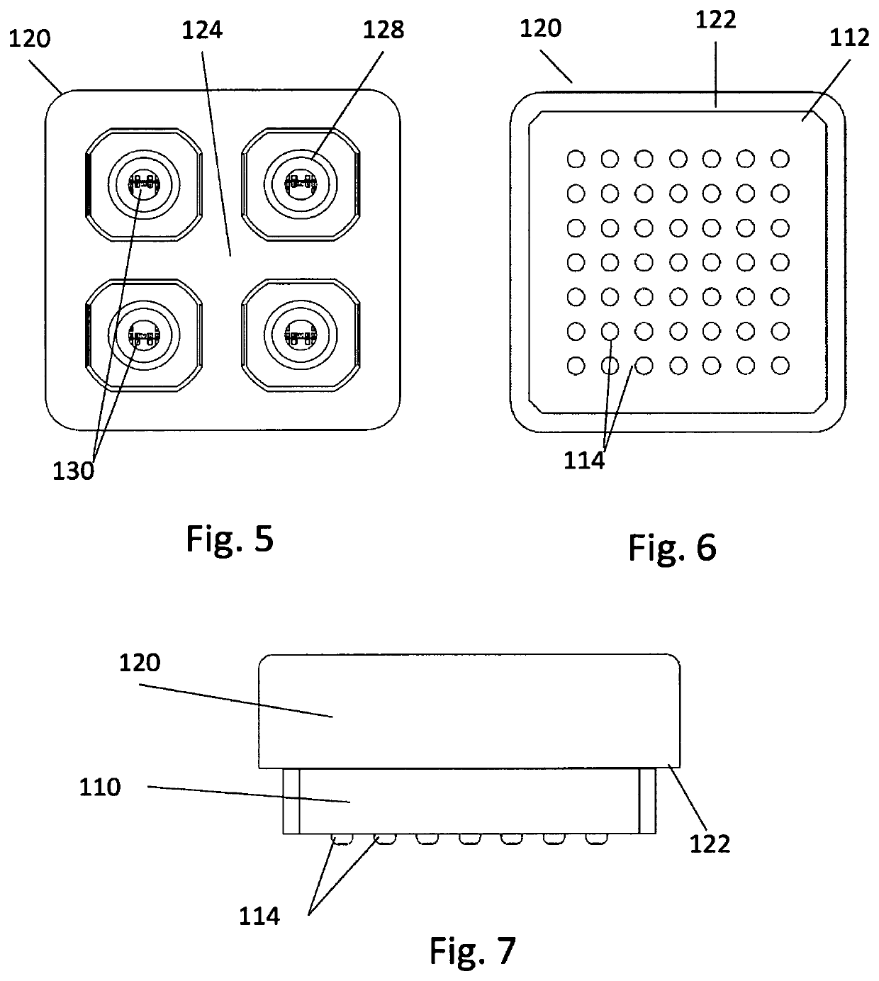
[0081]FIG. 2 shows an exploded isometric view of the components of the assembly 10 comprising the electro-optical module 100 and the optical connector 200 shown in FIG. 1. The electro-optical module 100 has the form of a ceramic package, comprising a ceramic substrate 110 and a ceramic cap 120, which contains an array of a plurality of electro-optical integrated circuit devices (e.g. see FIG. 4, electro-optical integrated circuit devices 130). On the front...

second embodiment

[0097]FIG. 14 shows a simplified cross-sectional view of parts of an assembly 1000 of the second embodiment comprising a fiber optic connector 1200 and an electro-optic module 1100 in the form of a CBGA package mounted on a circuit board 1102, wherein the connector 1200 is inserted into the electro-optic module 1100 and latched together with latches 1204 engaging latch apertures 1122 in the metal sleeve 1208. As illustrated schematically, the faces of the optical fibers are positioned a predetermined vertical distance z from the optical aperture of the photonic device for effective optical coupling. Numbering of other components of the assembly is the same as FIG. 13.

[0098]Depending on how the array of semiconductor devices are mounted on the substrate, the optical ports of the package are positioned to receive ferrules of the optical fibers with proper alignment in the lateral x-y direction and in the vertical z direction. This optical alignment will now be described in more detail...


PUM

PropertyMeasurementUnit
distancesaaaaaaaaaa
thicknessaaaaaaaaaa
diameteraaaaaaaaaa

Abstract

An electro-optical module is provided in the form of a Ceramic Ball Grid Array (CBGA) optical package with a detachable fiber optic connector. The electro-optical module is surface mountable on a printed circuit boards (PCB) using standard electronics pick-and-place and reflow manufacturing technology. A module housing array of ultra-high-speed single mode fiber based optical transmit and / or receive devices provides for high density fiber interconnections and can be mounted directly on a PCB in close proximity to associated electronics. The resulting shorter electrical interconnects reduce losses and distortion of the high frequency electrical signals enabling lower power signals and lower error rates on the interfaces, for applications such as high-speed data center interconnects. Shorter electrical interconnects may also allow for simpler clock and data recovery circuits or, in some cases, complete elimination of some of these circuits.

Description

CROSS-REFERENCE TO RELATED APPLICATIONS[0001]This application claims priority from U.S. provisional patent application No. 62 / 625,291 filed Feb. 1, 2018 entitled “Surface Mount Packaging for Single Mode Electro-Optical Module”, which is incorporated herein by reference in its entirety.TECHNICAL FIELD[0002]The present invention relates to packaging and interconnection of electro-optical devices comprising optical transmitters and receivers, such as single mode fiber based optical transmitters and receivers for data center applications.BACKGROUND[0003]High performance optical devices have conventionally been packaged in either pluggable packages that insert into the faceplate of the circuit boards of data switching equipment or in large modules that mount directly on circuit boards for long haul / high performance applications.[0004]In earlier times, data center interconnect was predominantly copper based. Interconnect speeds up to 1 GB / s were easily and cheaply implemented in small sil...

Claims


Application Information

Patent Timeline
Patent Type & Authority Patents(United States)
IPC IPC(8): G02B6/42G02B6/38G02B6/43H04B10/50H04B10/60H04B10/40
CPCG02B6/4292G02B6/3878G02B6/421G02B6/428G02B6/4249G02B6/4285G02B6/43G02B6/4228G02B6/4238G02B6/4245G02B6/4246H04B10/40H04B10/50H04B10/60H01L2224/73265H01L2224/48227H01L2224/48091H01L2224/05554H01L2924/00014
Inventor HJARTARSON, GUDMUNDUR A.ELLIOTT, CRAIG
Owner ELECTROPHOTONIC IC INC
Why Eureka
Try Eureka