Fabrication of a high density long channel dram gate with or without a grooved gate

Inactive Publication Date: 2001-06-07
IBM CORP
View PDF0 Cites 59 Cited by
  • Summary
  • Abstract
  • Description
  • Claims
  • Application Information

AI Technical Summary

Benefits of technology

[0013] Accordingly, the present invention lengthens gate conductors used in memory devices to limit leakage current, while still allowing the overall size of cells to remain the same. The channel length for each gate is increased by decreasing the size of spaces between gates. Decreases in space size occurs by using photolithographic image enhancement techniques. These techniques allow the space between gate conductors to be smaller while the gate size increases. In addition, a groove may be added that additionally lengthens the effective channel length and provides an additional electrical shield to limit leakage current. These techniques lead to the same density memory cells for a given process with less leakage. Finally, if grooved gate structures are used, having a longer gate conductor allows a three sigma process to be used, which increases yields.

Problems solved by technology

Problems can arise with decreasing DRAM cell size, however.
One important and potentially very serious problem is the associated decrease in capacitance that generally follows a decrease in cell size.
But it takes some time for the refresh circuitry to access and refresh each cell in the array, particularly when more cells are placed into an array.
Each cell must maintain its charge until refreshed, and this time period could be quite long, particularly with DRAMs' increasing cell numbers and density.
In addition to lower capacitance, as cell sizes decrease, sub-threshold leakage tends to increase.
Many of the causes of leakage actually decrease as cells and gate sizes decrease, but one important cause of leakage increases.
Drain induced barrier lowering becomes the predominant cause of leakage as cell and gate size decrease.
This current leakage reduces the time that the capacitor will store a charge and can cause potential errors if charge from the capacitor is transferred to the bit line or vice versa.
Unfortunately, with increasing density of cells on a chip, the refresh circuitry will take longer to refresh each cell.
This causes each gate length, and the corresponding channel length under the gate, to also become small, which leads to increased sub-threshold leakage from DRAM capacitors.
Therefore, without a way to increase the length of the gates without increasing the size of cells, increasing density of cells in DRAMs will cause greater leakage current or errors and more complex and costly refresh circuitry to counteract the increased leakage.

Method used


Image

  • Fabrication of a high density long channel dram gate with or without a grooved gate
  • Fabrication of a high density long channel dram gate with or without a grooved gate
  • Fabrication of a high density long channel dram gate with or without a grooved gate

Examples


example 2

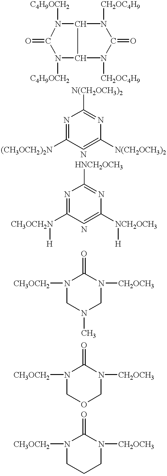
[0086] This example illustrates the manner in which changing the type of photoacid generator and relative amounts of the various components can change the dissolution rate characteristics of the hybrid resist and subsequently the lithographic response. This second formulation was prepared and processed in a manner similar to EXAMPLE 1, however, it is comprised of the following components:

[0087] PHS with about 25% of the phenol groups protected with MOP, 90.8% of solids;

[0088] triphenyl sulfonium triflate, 1.3% of solids;

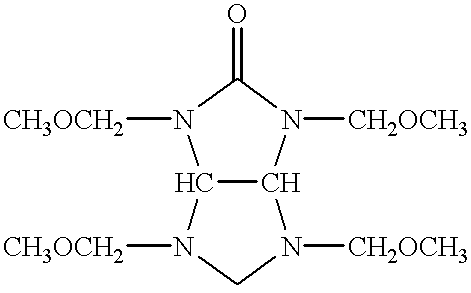
[0089] Powderlink, 7.8% of solids;

[0090] tetrabutyl ammonium hydroxide base, 0.1% of solids; and

[0091] sufficient PM acetate containing 350 ppm FC-430 surfactant as a solvent to form a 18.9% solids solution.

[0092] The dissolution rate characteristic of the resulting hybrid resist is shown in FIG. 14. The overall nature of the curve remains similar to that shown by the hybrid resist of EXAMPLE 1, in that the dissolution rate starts out low for an unexposed resist, inc...

example 3

[0094] This example illustrates that the space width of the frequency doubled image can be changed by varying the protection level of PHS with MOP. Two different PHS lots having 24% and 15% MOP loading, respectively, were used to make hybrid formulations identical to that of EXAMPLE 1, except that the total solids contents were adjusted to 16.0% of the total to obtain film thicknesses of about 0.5 .mu.m. From these two stock formulations, several other formulations with average MOP levels ranging from 15 to 24% were prepared. Wafers were coated and soft baked at 110.degree. C., exposed on a MICRASCAN II DUV 0.5 NA stepper, post exposed baked at 110.degree. C. for 60 sec and finally developed with 0.14N TMAH developer. A reticle with an isolated chrome opening was printed in a hybrid resist film. The spacewidth of the resist image was measured and graphed as a function of the average MOP solubility inhibitor loading in the PHS used for making the respective formulations. It was found...

example 4

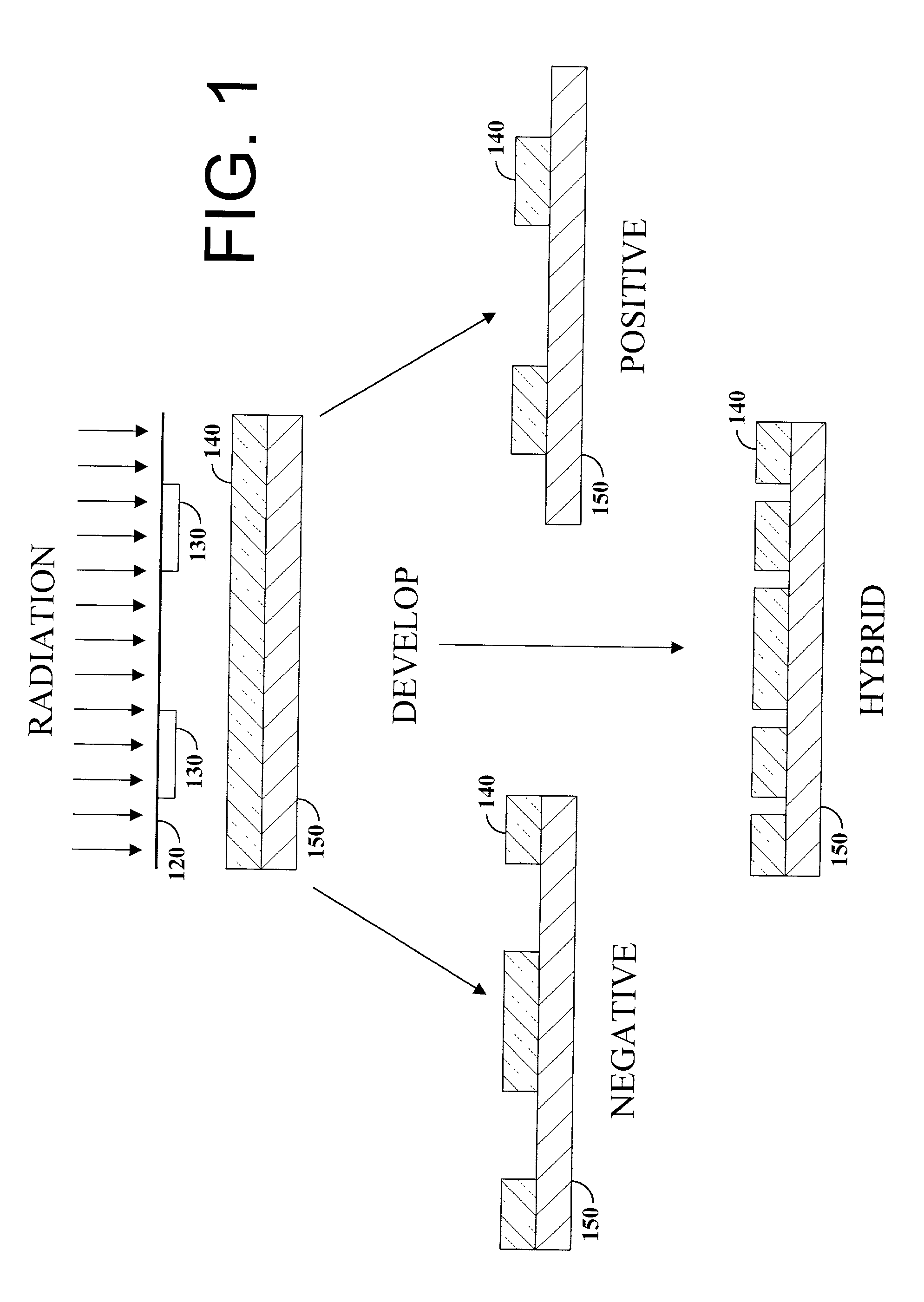
[0095] Negative tone imaging may be performed with the hybrid resist of the present invention, using a blanket DUV expose after the PEB and prior to the develop.

[0096] A hybrid resist formulation as described in EXAMPLE 2, above, was image-wise exposed with a chrome reticle with an electrical test pattern on a 0.5 NA DUV expose system. Silicon wafers (200 mm) with a 2000 Angstrom (.ANG.) film of polysilicon were used as a substrate so that the resulting etched patterns of the resist image could be measured with electrical probe techniques. After the post expose bake process, the wafers were cycled back into the expose tool (MICRASCAN II) and exposed at 10 mJ per square centimeter (cm.sup.2) with a clear glass reticle. A post expose bake process was not performed after the second exposure. The purpose of the second exposure was to remove the initially unexposed resist from the wafer, leaving only a negative tone resist pattern after develop.

[0097] The initial image-wise expose dose w...


PUM


Abstract

The present invention lengthens gate conductors used in memory chips to limit leakage current, while still allowing the overall size of cells to remain the same. The channel length for each gate is increased by decreasing the size of spaces between gates. Decreases in space size occurs by using photolithographic image enhancement techniques. These techniques allow the space between gate conductors to be smaller while the gate size increases. In addition, a groove may be added that additionally lengthens the effective channel length and provides an additional electrical shield to limit leakage current. These techniques lead to the same density memory cells for a given process with less leakage. Finally, if grooved gate structures are used, having a longer gate conductor allows a three sigma process to be used, which increases yields.

Description

[0001] This application is related to an earlier filed application by Furukawa et al., entitled "DRAM Cell with Grooved Transfer Device", Ser. No. ______, filed ______, and is incorporated herein by reference.[0002] 1. Technical Field[0003] The present invention relates generally to the field of semiconductor manufacturing and, more specifically, to forming long-channel gates, with or without grooves, in high-density Dynamic Random Access Memories (DRAM).[0004] 2. Background Art[0005] The need to remain cost and performance competitive in the production of semiconductor devices has caused continually increasing device density in integrated circuits. To facilitate the increase in device density, new technologies are constantly needed to allow the feature size of these semiconductor devices to be reduced.[0006] The push for ever increasing device densities is particularly strong in Dynamic Random Access Memory (DRAM) technologies, as more computers and peripherals come with higher amo...

Claims


Application Information

Patent Timeline
IPC IPC(8): H01L21/308H01L21/311H01L21/3213H01L21/8242H01L27/108
CPCH01L21/308H01L21/31144H01L21/32139H01L27/10829H01L27/10873H01L27/10876H10B12/37H10B12/05H10B12/053
Inventor FURUKAWA, TOSHIHARUHAKEY, MARK C.HOLMES, STEVEN J.HORAK, DAVID V.RABIDOUX, PAUL A.
Owner IBM CORP
Why Eureka
Try Eureka