Polishing silicon wafers

a belt-type apparatus and silicon wafer technology, applied in the direction of edge grinding machines, manufacturing tools, other chemical processes, etc., can solve the problems of increasing the number of layers applied, the design size of such integrated chips is steadily decreasing, and the micro-circuits are produced ever smaller and increasingly complex, so as to achieve high tensile strength, low elongation, and high tension

Inactive Publication Date: 2001-10-25
ROHM & HAAS ELECTRONICS MATERIALS CMP HLDG INC
View PDF0 Cites 24 Cited by
  • Summary
  • Abstract
  • Description
  • Claims
  • Application Information

AI Technical Summary

Benefits of technology

0014] The fabric may be a substrate which is woven in endless form embodying yarns of high tensile strength and relatively low elongation.
0015] A fabric woven in endless form lacks the weak spots of a seam or splice, which is a great advantage as these belts operate under extremely high tension to prevent the formation of ripples or wrinkles.

Problems solved by technology

The designed size of such integrated chips is steadily decreasing and the number of layers applied, e.g. by lithography onto the silicon surface is rising, to produce ever smaller and increasingly complex micro-circuits.
This increase in the number of layers applied is leading to ever more stringent requirements on the smoothness and planarity of the silicon wafers, since pits or scratches may produce voids which cannot be bridged by deposited material, as the widths and thicknesses of deposited layers are decreased, leading to unplanned resistances where a conductor is narrowed, or capacitances / non-conductive gaps, where breaks occur in deposited conductor layers, which interfere with or compromise the planned operation of the circuit.
A major problem with these belts is the poor adhesion of polyurethane to steel.
An adhesive or coupling agent is required for bonding between the steel and polyurethane to take place but in spite of the use of such an agent bond strength is insufficient to withstand the harsh conditions under which the belt operates--particularly the frictional forces occurring between the belt and wafer in the zone of contact.
The tendency is for the polyurethane to wear out or to flake off within two days or so, and to repair this an area around the damaged coating has to be removed for fresh polyurethane to be added as a patch.

Method used


Image

  • Polishing silicon wafers
  • Polishing silicon wafers

Examples


Embodiment Construction

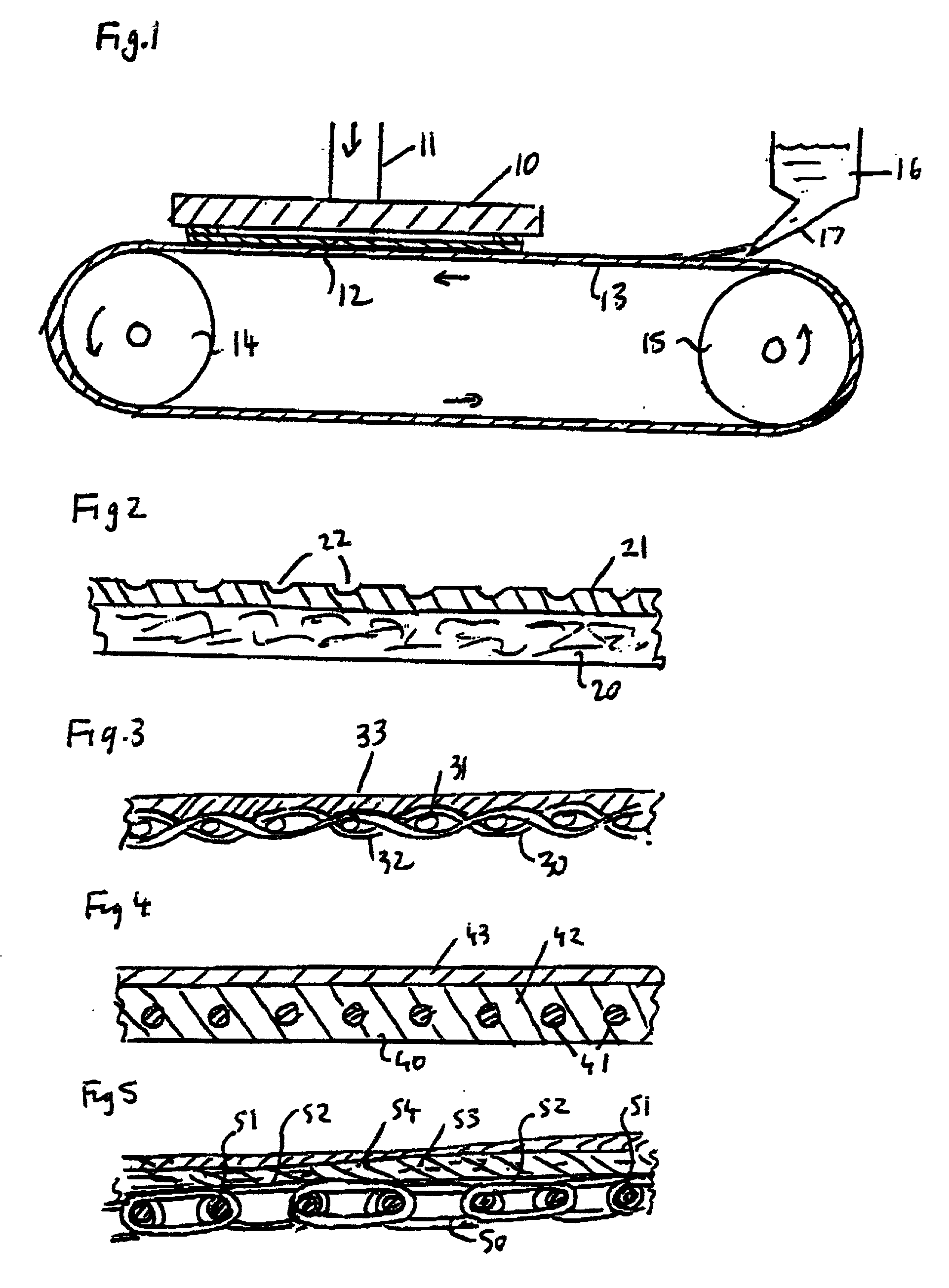
[0032] FIG. 1 is a diagrammatic view of a continuous belt machine for polishing and planarising silicon wafers. A platen 10 operable by a hydraulic or pneumatic ram 11, holds a silicon wafer 12 flat on the surface of a continuous belt 13, after the wafer 12 has been put in place by a remotely controlled or autonomous handling system such as a robotic arm (not shown). Belt 13 is passed around end rollers, 14, 15 and is driven in the sense indicated by the arrows on the drawing. A polishing slurry, containing very fine grade abrasive is fed onto the upper surface of the belt from a reservoir 16, through a feeder 17. An example of a suitable polishing slurry is disclosed in WO 96 / 16436 by Advanced Micro Devices, Inc. The feeder 17 may be associated with means known in the prior art for achieving the desired distribution of the slurry on the belt, prior to encountering the wafer 12 which is to be polished by the chemical-mechanical polishing process.

[0033] Polishing is achieved by the m...


PUM


Abstract

An endless belt for a belt type polishing machine comprises a support fabric and a polymer layer of relatively low hardness. The polymer layer is formed with drainage grooves. The support fabric may comprise a non woven or woven material, or a membrane with oriented reinforcing yarns. A further version comprises a spiral-link fabric supporting a woven or non woven layer carrying the polymer layer. The polymer layer may be a double layer, the upper of which is either harder or softer than the lower layer.

Description

[0001] This invention relates to apparatus for polishing silicon wafers.[0002] Silicon wafers are produced as precursors from which micro-electronic semiconductor components are produced. The wafers are grown for example by deposition of silicon onto a substrate, to produce discs typically 20 cm in diameter, which are split by cleavage parallel to their major surfaces (analogous to the cleavage of slate) to produce two thinner wafers. The resulting wafers require to be polished to give totally flat and planar surfaces for deposition of electronic components onto the surface by standard lithographic and etching techniques to form integrated chip semiconductor devices. Typically a 20 cm diameter wafer will produce forty micro processor chips.[0003] The designed size of such integrated chips is steadily decreasing and the number of layers applied, e.g. by lithography onto the silicon surface is rising, to produce ever smaller and increasingly complex micro-circuits. Present semiconduct...

Claims


Application Information

Patent Timeline
Patent Type & Authority Applications(United States)
IPC IPC(8): B24B21/04B24B37/20B24B37/26B24D11/06H01L21/304
CPCB24B21/04B24B37/205B24B37/26B24D11/06H01L21/304
Inventor DUDOVICZ, WALTER
Owner ROHM & HAAS ELECTRONICS MATERIALS CMP HLDG INC
Why Eureka
Try Eureka