Semiconductor device

a technology of semiconductor devices and semiconductors, applied in semiconductor devices, semiconductor/solid-state device details, capacitors, etc., can solve the problems of lowering yield, lowering reliability of semiconductor devices, etc., and achieve the effect of preventing breakag

Inactive Publication Date: 2001-11-22
HITACHI LTD
View PDF0 Cites 14 Cited by
  • Summary
  • Abstract
  • Description
  • Claims
  • Application Information

AI Technical Summary

Benefits of technology

[0021] The present inventors have made extensive studies to solve the aforementioned problems and have found that breads of tungsten interconnect, which is one of the problems to be solved by the present invention, proceeds by diffusion of tungsten atoms near the crystal grain boundary and further that, to control the grain boundary diffusion of the atoms in the tungsten wiring it is effective to add to the tungsten interconnect such an element as to narrow the interatomic distance of tungsten crystal in the tungsten interconnect (additive element).
[0023] In the semiconductor device of the foregoing structure, the interconnect can be prevented from breaking by using a metal interconnect composed of tungsten as the main constituent material and containing molybdem. Effective molybdenum content is 0.05 at %-18 at. %, preferably 0.1 at. %-15 at. %.

Problems solved by technology

However, when the aforementioned prior art was applied to semiconductor devices such as 256 M bit DRAM or system LSI (semiconductor device with memory LSI and logic LSI mounted together on a single chip), such problems as breaking of tungsten interconnects, lowering of semiconductor device reliability, lowering of yield, etc. were encountered in some cases.

Method used


Image

  • Semiconductor device
  • Semiconductor device
  • Semiconductor device

Examples


first embodiment

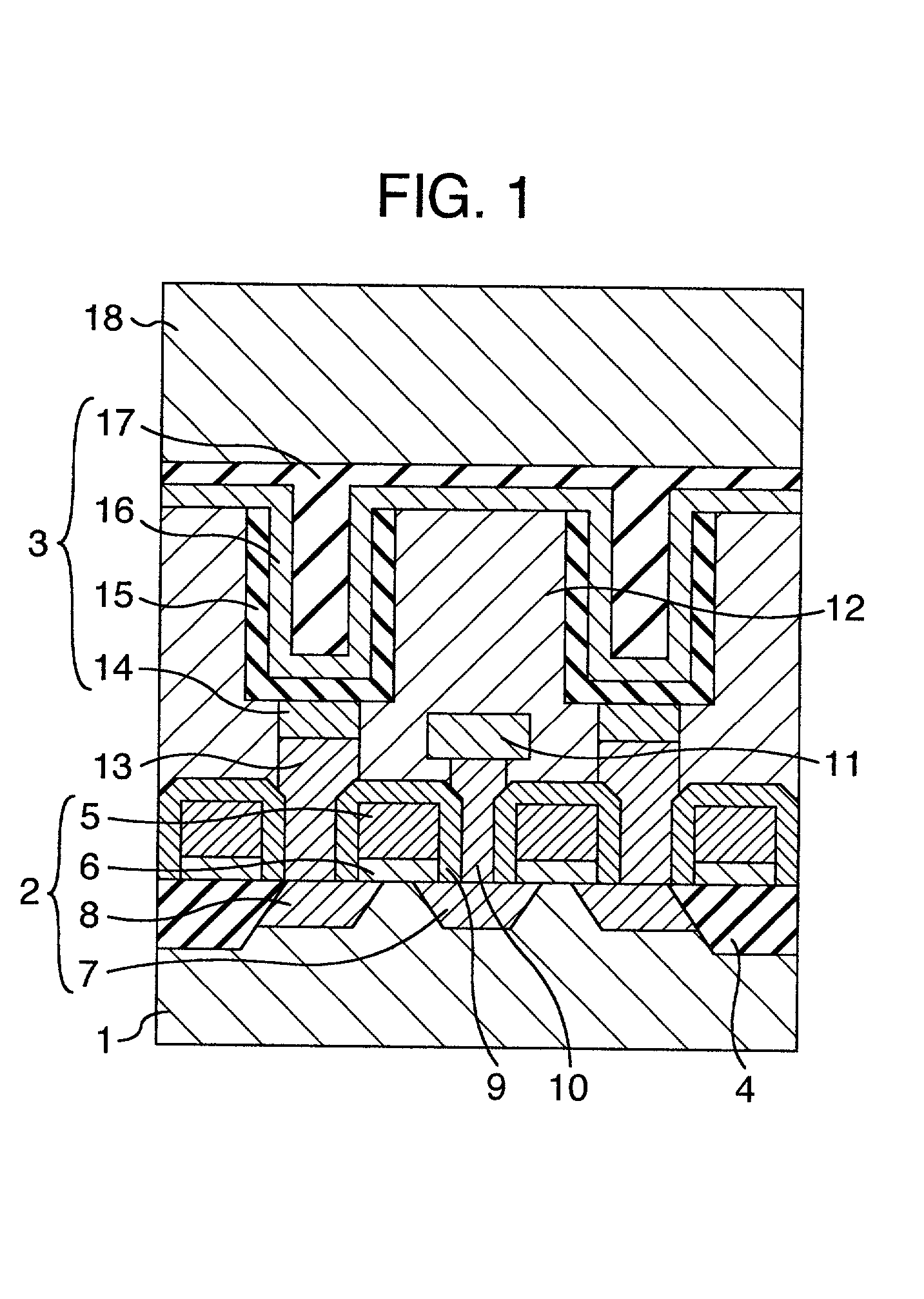
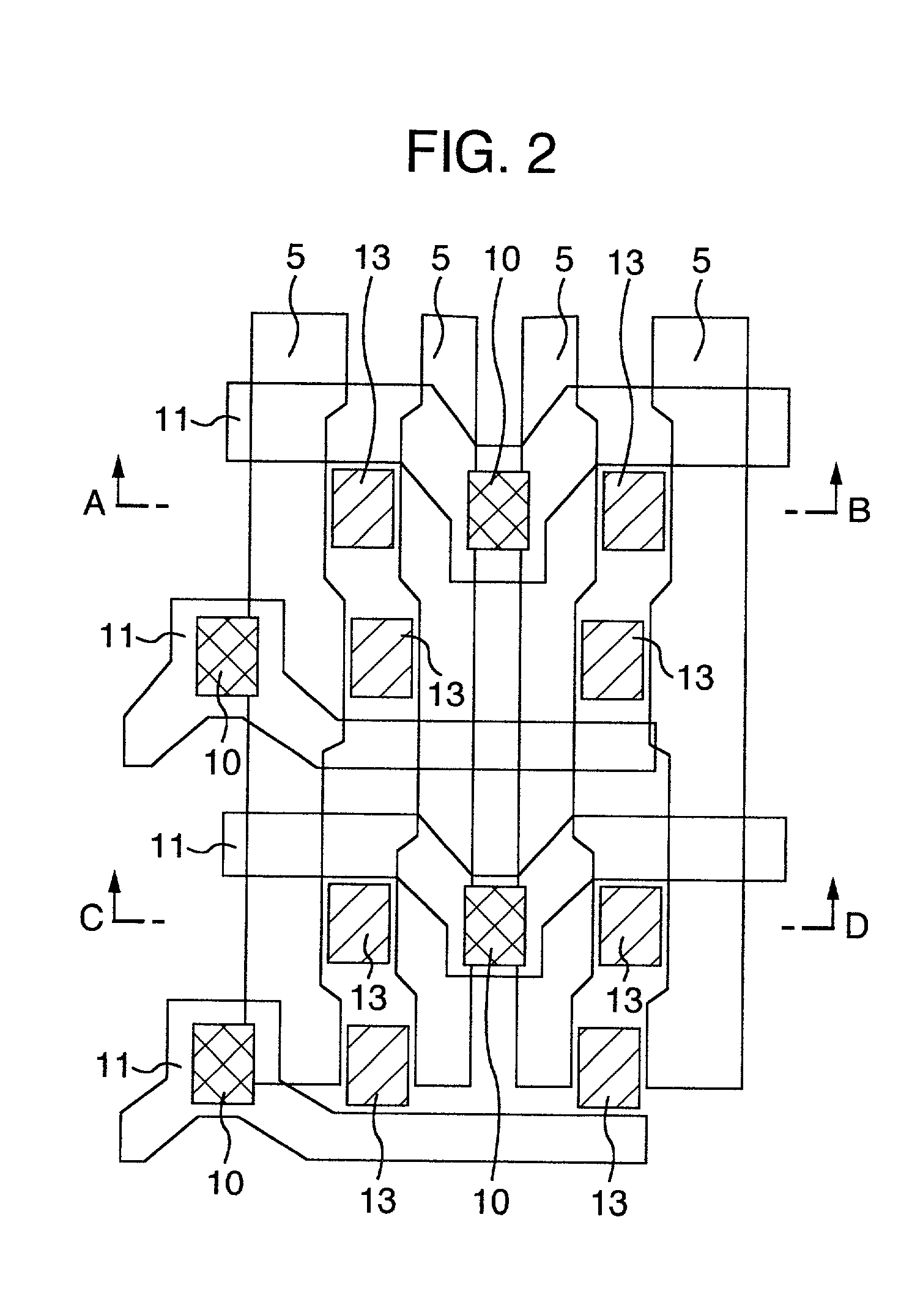
[0036] Cross-sectional structure of DRAM (Dynamic Random Access Memory) memory cell is shown in FIG. 1 as the present semiconductor device. FIG. 1 is a cross-sectional view along A-B or C-D in an example of plan layout shown in FIG. 2. The semiconductor device of this Example comprises a MOS (Metal Oxide Semiconductor) type transistor formed in the active region on the principal plane of silicon substrate 1 as a semiconductor and information storage capacitor component 3 (which may be hereinafter referred to as "capacitor component") provided thereon. Insulation film 12 is a film for isolation between components.

[0037] MOS transistor 2 of the memory cell comprises gate electrode 5, gate insulation film 6 and diffusion layer 7. Gate insulation film 6 consists of, for example, a silicon oxide film, a silicon nitride film or a ferroelectric film or is in a laminate structure of these films. Gate electrode 5 consists of, for example, a polycrystalline silicon film, a thin metal film, or...

example 2

[0045] Cross-sectional structure of DRAM memory cell is shown in FIG. 5 as a second embodiment of the present semiconductor device. FIG. 5 is also a cross-sectional view along A-B or C-D in an example of plan layout shown in FIG. 2. This embodiment differs from the first embodiment in conductive film 19 consisting, for example, of tungsten nitride or titanium nitride, formed below bit line 11. When plug 10 is composed of polycrystalline silicon as the main constituent element, there is such a risk that the silicon element diffusion into bit line 11 from plug 10, deteriorating device characteristics, and conductive film 19 thus acts as a barrier against such diffusion. One or more layers of another film may be provided between conductive film 19 and plug 10.

example 3

[0046] Cross-sectional structure of DRAM memory cell is shown in FIG. 6 as a third embodiment of the present invention. FIG. 6 is also a cross-sectional view along A-B or C-D in an example of plan layout shown in FIG. 2. the third embodiment differs from the first embodiment in conductive film 20 formed on the bottom and sides of bit line 11 so as to make breaking of bit line 11 much less. Though not shown in the drawing, the conductive film as a barrier as shown in the second embodiment may be formed under conductive film 20 an overlay film may be provided on the top of bit line 11 so as to make breaking much less.


PUM

PropertyMeasurementUnit
widthaaaaaaaaaa
temperatureaaaaaaaaaa

Abstract

In a semiconductor device, which comprises a capacitor component comprising a first electrode, an oxide film with a high dielectric constant or ferroelectricity in contact with the first electrode and a second electrode in contact with the oxide film, as formed in this order, on one principal side of a silicon substrate with a metal wiring layer formed thereon, such problems as breaking of tungsten interconnect, lowering of reliability, lowering of yield, etc. of semi-conductor devices can be solved by using molybdenum-containing tungsten as the material of metal interconnect layer.

Description

[0001] The present invention relates to a semiconductor device and a process for producing the same.[0002] With the recent trend toward finer semiconductor devices, the area of information storage capacitor component has become smaller and smaller and the absolute value of capacitance has also become smaller and smaller. In case of a parallel flat plate electrode structure, a capacitance C can be defined by the following equation:C=.di-elect cons..multidot.S / d[0003] where .di-elect cons. is a permittivity of dielectric, S an area of electrode and d a film thickness (interelectrode distance) of dielectric. To secure a capacitance without increasing the area S of electrode used in the information storage capacitor component, it is necessary to use a dielectric material with a high permittivity .di-elect cons. or make the film thickness d of dielectric smaller. The thickness of a thin oxide film is now made as small as about 10 nm, and in case of memory of high integration level of 64 ...

Claims


Application Information

Patent Timeline
Patent Type & Authority Applications(United States)
IPC IPC(8): H01L21/02H01L21/8242H01L21/8246H01L23/532H01L27/105H01L27/108
CPCH01L23/53257H01L27/10814H01L27/10894H01L28/55H01L2924/0002H01L28/60H01L2924/00H10B12/315H10B12/09H10B12/00
Inventor IWASAKI, TOMIOMIURA, HIDEONAKAJIMA, TAKASHIOHTA, HIROYUKINISHIHARA, SHINJISAHARA, MASSASHI
Owner HITACHI LTD
Why Eureka
Try Eureka