
Method of manufacturing thin film transistor

Inactive Publication Date: 2002-06-13
GOLD CHARM LTD
View PDF0 Cites 6 Cited by
  • Summary
  • Abstract
  • Description
  • Claims
  • Application Information

AI Technical Summary

Benefits of technology

[0020] Still another object of the invention is to provide a thin film transistor which guarantees: using the chemical vapor deposition (CVD), which enables good step-coverage precision, and particularly plasma CVD rather than the physical vapor deposition, which is represented by sputtering high in directivity and not suitable in covering the stepped edges of the island, (1) lowering the defect level derived from residual stress, dangling bond, impurity, etc. and improving the insulating strength, (2) lowering the interface level derived from incomplete cleaning, plasma damage, etc., and (3) covering stepped edges of the island of semiconductor layers precisely.

Problems solved by technology

However, in the polysilicon TFT technology, inexpensive low-melting-point glass, which is originally suitable to the former process, cannot be employed in the above-mentioned high-temperature process.
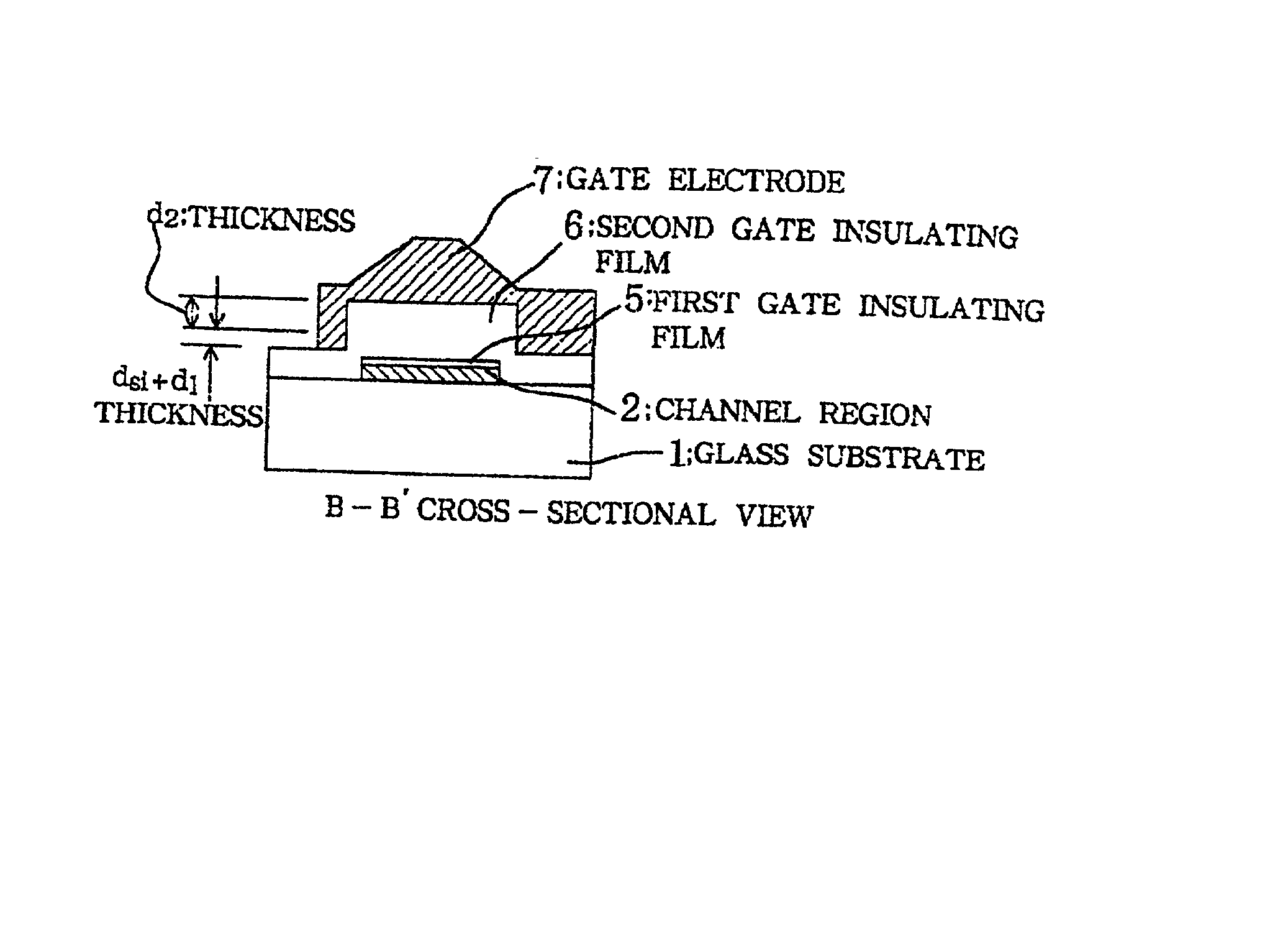
Consequently, if the gate insulating film is thinned in order to lower the threshold voltage as mentioned above, then the thickness of the second gate insulating film becomes smaller than the difference between the semiconductor layer and the first gate insulating film so that gate-leak-free covering is difficult to achieve.
Thus short circuit (gate leak) would tend to occur between the gate and the source-and-drain region.
However, this publication is totally silent about and even does not anticipate any second insulating film that covers the stepped edges of the island constituted by the semiconductor layer and the first gate insulating film.
However, in sputtering, since the film-forming precursor strikes on the substrate at about right angles, precise covering over the stepped edges of the island is difficult to achieve.
In this conventional method, however, although a good interface can be formed, the insulating strength is yet low so that thinning of the gate insulating film in an effort to secure the necessary reliability of the device and to lower the threshold voltage would be difficult to achieve.

Method used


Image

  • Method of manufacturing thin film transistor
  • Method of manufacturing thin film transistor
  • Method of manufacturing thin film transistor

Examples


embodiment 1

[0061] [Embodiment 1]

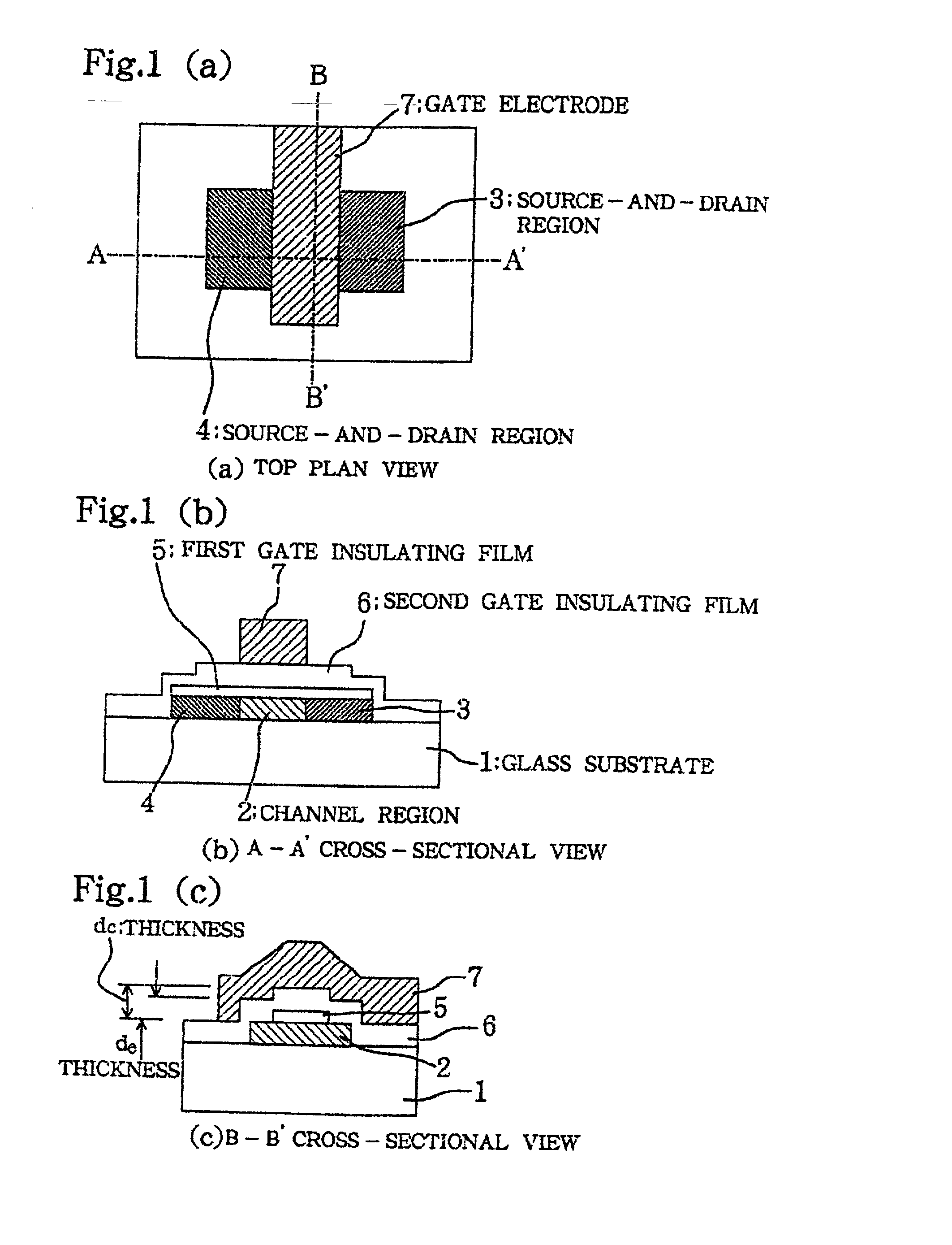
[0062] FIG. 1(a) is a top plan view of a thin film transistor according to a first embodiment of the invention, FIG. 1(b) is a cross-sectional view taken alone line A-A' of FIG. 1(a), and FIG. 1(c) is a cross-sectional view taken alone line B-B' of FIG. 1(a). The thin film transistor of FIGS. 1(a) to 1(c) comprises a glass substrate 1 as an insulator, and a silicon layer composed of a source-and-drain region 4, 3, and a channel region 2 and formed on the glass substrate 1 in an island shape. A first gate insulating film 5, which is formed on the island of the silicon layer, has a first width equal to the width of the silicon layer in the source-drain direction, i.e., the B-B' direction and a second width smaller than the width of the silicon layer in the gate electrode direction, i.e., in the B-B' direction. In the gate electrode direction, a below-described gate electrode extends across the first-gate insulating film 5. These regions of the silicon layer and th...

embodiment 2

[0069] [Embodiment 2]

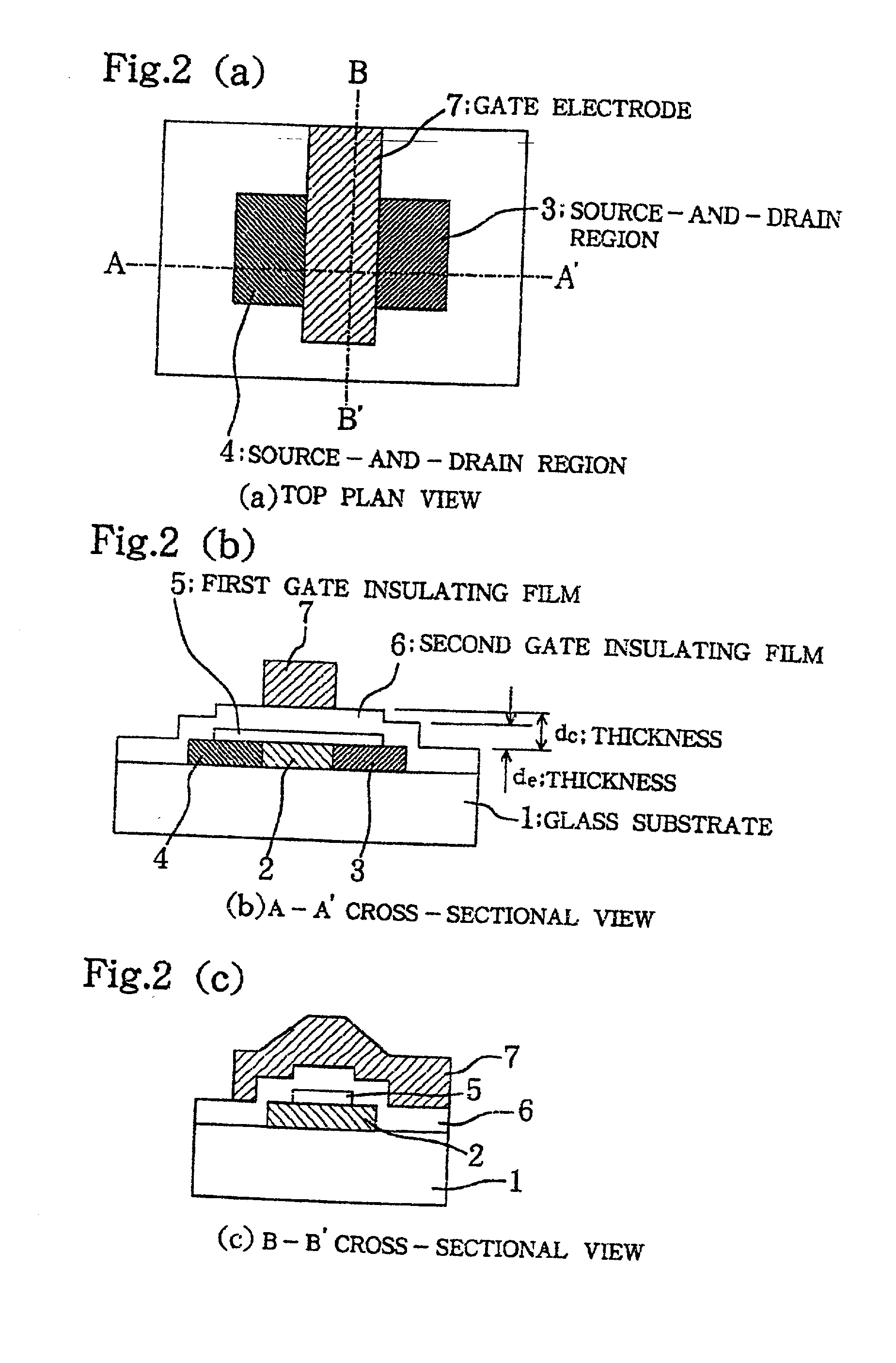
[0070] FIG. 2(a) is a top plan view of a thin film transistor according to a second embodiment of the present invention, FIG. 2(b) is a cross-sectional view taken alone line A-A' of FIG. 2(a), and FIG. 2(c) is a cross-sectional view taken alone line B-B' of FIG. 2 (a). The thin film transistor of FIGS. 2(a) to 2(c) comprises a glass substrate 1 as an insulator, a silicon layer, which is composed of a source-and-drain region 4, 3 and a channel region 2 and formed on the glass substrate 1 in an island shape, a first gate insulating film 5, a second gate insulating film 6, and a gate electrode (hereinafter also called the gate) 7. Because the channel region 2, the gate insulating films 5, 6 and the gate 7 constitute the so-called metal-insulator-semiconductor structure, it is possible control a drain current by controlling a voltage applied to the gate 7. The material for the first and second gate insulating films 5, 6 is exemplified by silicon dioxide, silicon nit...

embodiment 3

[0076] [Embodiment 3]

[0077] FIGS. 3(a) is a top plan view of a thin film transistor according to a third embodiment of the present invention, FIG. 3(b) is a cross-sectional view taken alone line A-A' of FIG. 3(a), and FIG. 3(c) is a cross-sectional view taken alone line B-B' of FIG. 3(a). The thin film transistor of FIGS. 3(a) to 3(c) comprises a glass substrate 1 as an insulator, a silicon layer, which is composed of a source-and-drain region 4, 3 and a channel region 2 and formed on the glass substrate 1 in an island shape, a first gate insulating film 5, a second gate insulating film 6, and a gate electrode 7. Because the channel region 2, the gate insulating films 5, 6 and the gate 7 constitute the so-called metal-insulator-semiconductor structure, it is possible control a drain current by controlling a voltage applied to the gate 7. The material for the first and second gate insulating films 5, 6 is exemplified by silicon dioxide, silicon nitride, aluminum oxide and tantalum ox...


PUM


Abstract

In a thin film transistor, a first insulating film on a silicon layer formed in an island on a substrate is smaller in thickness than the silicon layer so that the stepped island edges is gentle in slope to facilitate covering the island with a second insulating film. This reduces occurrence of gate leak considerably. Since the peripheral region of the stepped island is smaller in thickness than the central region above the channel, it is possible to minimize occurrence of gate electrode breakage. The silicon layer contains two or more inert gas atoms, and the atoms smaller in mass number (e.g., He) are contained in and near an interface with a silicon active layer while the atoms larger in mass number (e.g., Ar) than those smaller in mass number are contained in and near a second interface with a gate electrode.

Description

[0001] 1. Field of the Invention:[0002] The present invention relates to a thin film transistor for use in an active matrix liquid crystal display panel, an input / output device as of a contact-type image sensor, a portable electronic instrument, etc., and also to a method for manufacturing such thin film transistor.[0003] 2. Description of the Related Art:[0004] In forming a thin film transistor (hereinafter also called TFT) on a substrate of glass, the hydrogenated amorphous silicon semiconductor TFT technology and the polysilicon TFT technology are currently available as typical technologies. According to the former, the maximum temperature of the fabrication process is about 300.degree. C., and a carrier mobility of approximately 1 cm.sup.2 / Vsec is obtained. According to the latter, using a high-temperature process analogous to the LSI process of about 1000.degree. C. using a substrate as of quartz, a carrier mobility of 30 to 100 cm.sup.2 / Vsec can easily be obtained. In case of ...

Claims


Application Information

Patent Timeline
IPC IPC(8): H01L21/00H01L21/339H01L21/4763H01L21/84H01L27/01H01L27/12H01L31/0392
CPCH01L27/14665H01L29/78609H01L29/66757H01L29/42384
Inventor TANABE, HIROSHIYUDA, KATSUHISAOKUMURA, HIROSHISATO, YOSHINOBU
Owner GOLD CHARM LTD
Learn More