Electronic device with composite substrate

a composite substrate and electronic device technology, applied in the direction of single crystal growth, polycrystalline material growth, chemistry apparatus and processes, etc., can solve the problems of relatively high thermal impedence, high cost of single crystal sic substrate, and growth of high-quality sic epitaxial layers on silicon substrates. achieve improved thermal expansion, improve microwave insulating characteristics, and improve thermal conduction

Inactive Publication Date: 2002-07-25
THE GOVERNMENT OF THE UNITED STATES OF AMERICA AS REPRESENTED BY THE SEC OF THE NAVY NAVAL RES LAB WASHINGTON
View PDF0 Cites 92 Cited by
  • Summary
  • Abstract
  • Description
  • Claims
  • Application Information

AI Technical Summary

Benefits of technology

0021] Another object of this invention is structures and methods to make a composite substrate with improved thermal conduction, improved thermal expansion, improved microwave insulating characteristics, improved electrical conductivity and / or improved optical transmission properties, to which a single crystal material layer is direct wafer bonded and on which at least one epitaxial layer is grown.
0022] Another object of this invention is the methods to laterally isolate regions of the composite substrate so that stresses generated in one polycrystalline substrate layer due to differences in thermal expansion between the layers of a composite substrate do not cause excessive stress in the single-crystal layer that is direct wafer bonded to the composite substrate and the epitaxial layer that is grown on the single-crystal layer.

Problems solved by technology

However, single crystal SiC substrates are very expensive and are currently available in small substrate sizes.
However, the large lattice mismatch (.about.20%) and thermal expansion mismatch (.about.8%) between SiC and silicon have to date prevented the growth of high quality SiC epitaxial layers on silicon substrates.
An additional problem with this approach is that the optimum growth temperature for SiC epitaxial growth is between 1500.degree. C. and 1600.degree. C., well above the 1350.degree. C. maximum use and the 1450.degree. C. melting temperature of a silicon substra
Sapphire is electrically insulating, a disadvantage for vertical current conducting optical emitters and power devices, and has relatively high thermal impedence which is a disadvantage for high power microwave devices.
The best quality GaN epitaxial layers have been obtained for material grown on SiC substrates, however, single crystal SiC substrates are very expensive and are only available in small substrate sizes.
There is however, significant thermal expansion mismatch between GaN and silicon which leads to cracking of the epitaxial layer for thick GaN epitaxial layers.
The silicon substrate is not suitable for microwave applications because of the microwave loss in the conducting silicon substrate.
There is also a significant lattice mismatch between GaN lattice and silicon lattice, however, GaN epitaxial layers with reasonable electron mobilities have been grown on a silicon substrate.

Method used


Image

  • Electronic device with composite substrate
  • Electronic device with composite substrate
  • Electronic device with composite substrate

Examples


example ii

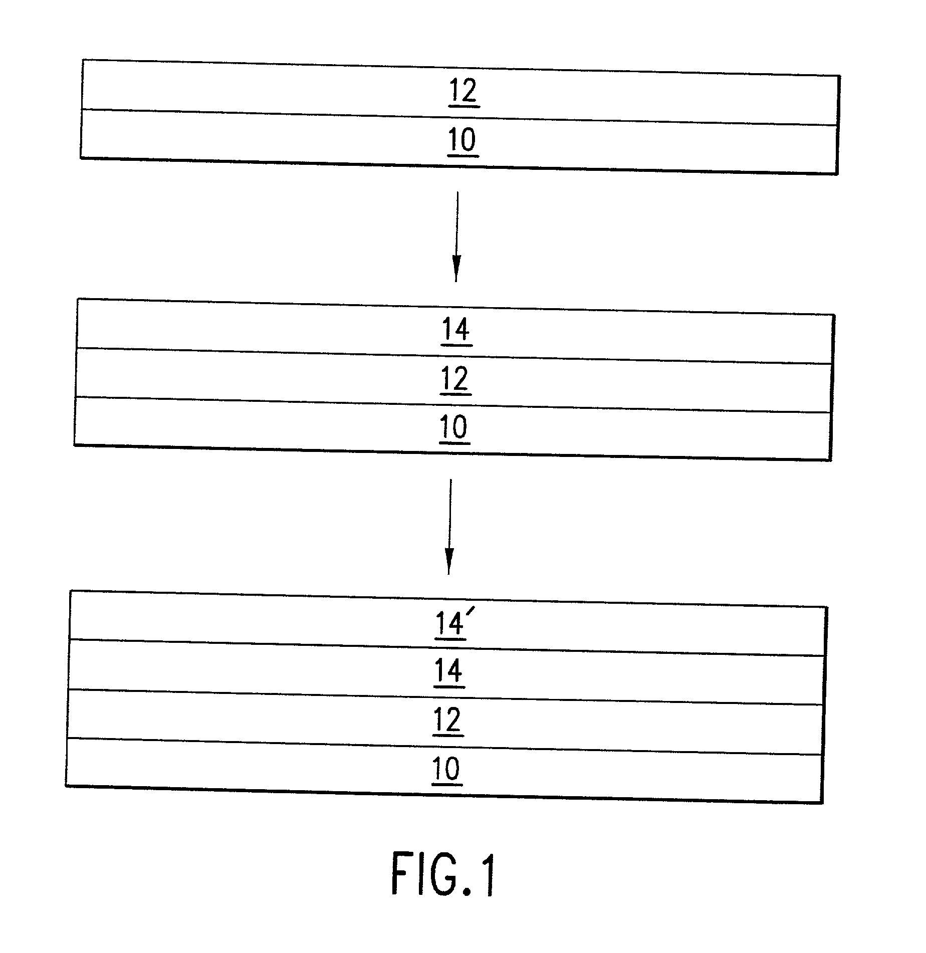
[0078] Example of AlN / GaN growth on diamond / AlN ceramic composite substrate.

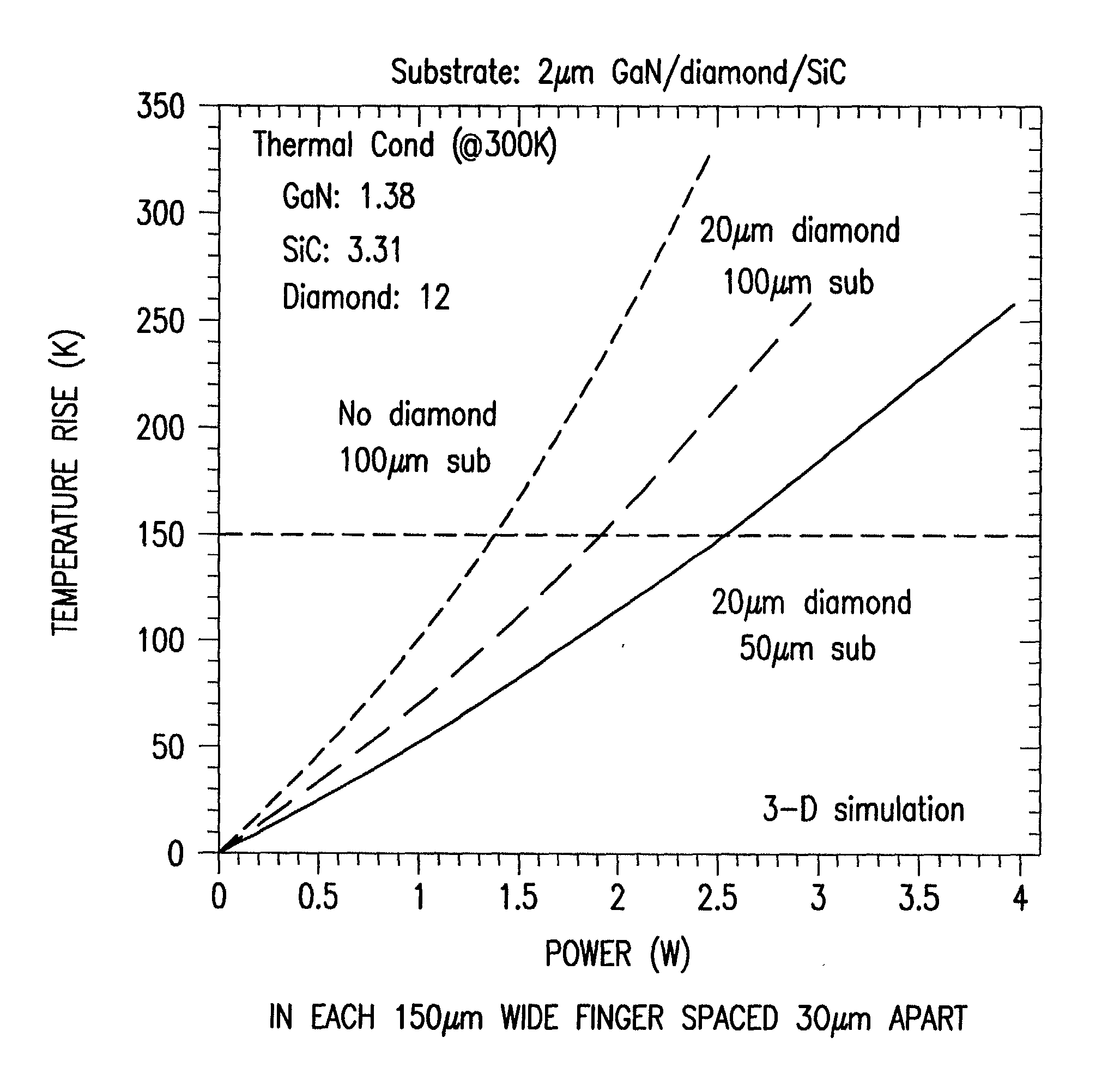
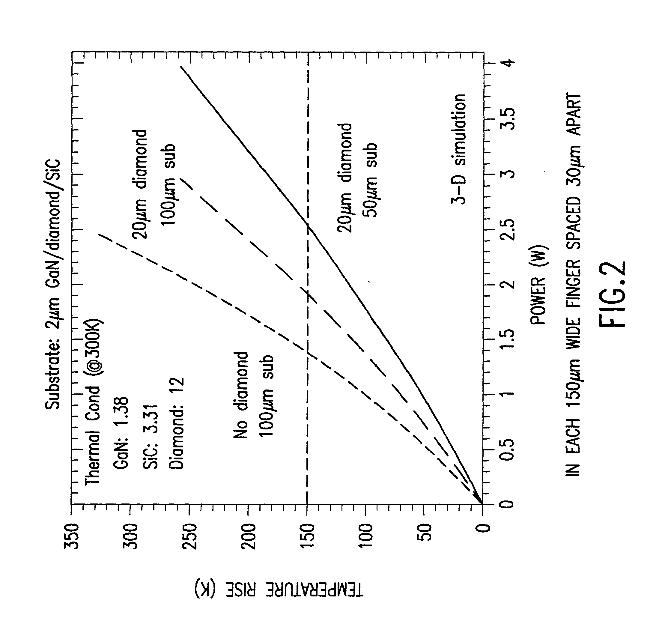
[0079] 1. Select a ceramic AlN substrate because of the excellent thermal expansion match between ceramic AlN and AlN / GaN epitaxial layer and also because of the excellent thermal conductivity and microwave insulation properties. A good alternate substrate is poly-SiC which also have good thermal expansion match to AlN / GaN epitaxial layer and has a thermal conductivity of approximately 300 W / mK. An alternate approach for selecting the first substrate so that the equivalent thermal expansion coefficient of the composite close to that for the AlGaN / GaN epitaxial layer. Since diamond has a thermal expansion of 2.3.times.10.sup.-6 and the thermal expansion coefficient of the AlGaN / GaN epitaxial layer is approximately 4.6.times.10.sup.-6, it is necessary to choose the thermal expansion coefficient of the first substrate to be higher than 4.6.times.10.sup.-6 so that the equivalent thermal expansion is closer to th...


PUM

PropertyMeasurementUnit
temperatureaaaaaaaaaa
strain point temperatureaaaaaaaaaa
melting temperatureaaaaaaaaaa

Abstract

A method for making a multilayered electronic device with at least one epitaxial layer grown on a single-crystal film bonded to a composite wherein at least one layer is polycrystalline, the method includes the step of bonding a single-crystal film at least one of the epitaxial layers on the single-crystal film wherein thermal coefficients of expansion for the substrate and the epitaxial layer are closely matched.

Description

REFERENCE TO RELATED APPLICATION[0001] This patent application is an improvement over the application entitled "Single Crystal Material on Non-Single-Crystalline Substrate" which was filed Feb. 1, 1999 and bears Ser. No. 09 / 243, 182.[0002] 1. Field of the Invention[0003] This invention pertains to an electronic device containing a composite substrate which is a multi-layer of which at least one layer is polycrystalline, and to a method for making same.[0004] 2. Description of Related Art[0005] A large area, inexpensive substrate for the growth of epitaxial layers gallium nitride (GaN) and silicon carbide (SiC) has been a long-sought goal. Currently, single crystal GaN and SiC substrates are the predominantly used substrates for epitaxial growth. However, single crystal SiC substrates are very expensive and are currently available in small substrate sizes. For instance, 8" polycrystalline SiC substrates are available for about $800 whereas the largest single-crystal SiC substrate ava...

Claims


Application Information

Patent Timeline
Patent Type & Authority Applications(United States)
IPC IPC(8): H01L21/20
CPCH01L21/2007Y10S117/915
Inventor KUB, FRANCIS J.HOBART, KARL D.
Owner THE GOVERNMENT OF THE UNITED STATES OF AMERICA AS REPRESENTED BY THE SEC OF THE NAVY NAVAL RES LAB WASHINGTON
Why Eureka
Try Eureka