Multi-layer wiring substrate

a wiring substrate and multi-layer technology, applied in the field of multi-layer wiring substrates, can solve the problems of difficult to form through-holes having a uniform pore diameter, difficult to achieve the effect of uniform dielectric layer separation, and limited through-hole minuteness

Inactive Publication Date: 2002-11-21
KYOCERA CORP
View PDF0 Cites 53 Cited by
  • Summary
  • Abstract
  • Description
  • Claims
  • Application Information

AI Technical Summary

Problems solved by technology

However, in the dielectric layer made up of impregnating the epoxy resin in the glass cloth, there is a difficulty in providing a hole in the glass cloth by a laser whereby there is a limitation on minuteness of the through-hole and, further, there is a problem that it is difficult to form the through-hole having a uniform pore diameter due to the fact that a thickness of the glass cloth is not uniform.
However, the insulating backing material using the aramid non-woven fabric or the polyimide film is highly hygroscopic whereupon there is a problem that, when the insulating backing material which has absorbed moisture is subjected to a soldering reflow, the moisture absorbed therein is vaporized to generate a gas thereby causing a separation of the dielectric layer or other unfavorable phenomena.
Further, the epoxy-type adhesive is high in a dielectric constant whereupon there is another problem that transmission characteristics thereof in a high frequency region are deteriorated.
However, in the multi-layer printed circuit substrate proposed by JP-A 8-97565, when the adhesive layer containing the liquid crystal polymer is inserted between a plurality of circuit layers and adhered them with one another by means of thermal compression bonding, due to the fact that the liquid crystal polymer is rigid to be incapable of moving into a fine dent formed on a surface of the circuit layer, there is a problem that it can not exert a sufficient anchor effect whereupon adhesiveness between the circuit layer and the adhesive layer is inferior to exhibit an insulation failure by a high temperature bias test.
Further, in the high-frequency circuit substrate proposed by JP-A 2000-269616, since a dielectric constant of the epoxy-type adhesive is different from that of the liquid crystal polymer to a great extent, by a small variation of thickness to be caused by a pressure to be applied at the time of lamination, there appears a problem that the transmission characteristics are deteriorated in the high frequency region, particularly, in a frequency region of 100 MHz or more.
Further, since a film in which an orientation property of liquid crystal polymer molecules is corrupted is used, an attraction force between the liquid crystal polymer molecules becomes weak whereby coefficient of thermal expansion of liquid crystal polymer film is increased and, as a result, when the multi-layer wiring substrate is constituted by these substrates, there is a problem that a wiring failure is generated at a joint between a through-hole conductor and a wiring conductor therein by a temperature cycle test.
Further, in accordance with a weak attraction force between the molecules, flexural strength becomes weak whereupon there is a problem that, when the wiring substrate is brought to be thinner than before by decreasing a thickness of the electric dielectric layer, a camber will be generated therein.
Further, since a content of the inorganic insulating fillers in the third layer is set to be as small as from 20% by volume to 40% by volume, there neither occurs a case in which adhesiveness between the cladding layer and the wiring conductor is deteriorated to prevent the wiring conductor from being adhere-formed on the cladding layer, nor a case in which, when the dielectric layers are adhered to each other, adhesiveness between the cladding layers to form the dielectric layer is deteriorated to generate a separation between the dielectric layers causing a deterioration of an insulating property thereof.
Further, when the thickness of the cladding layer 6 is less than 3 .mu.m, stress which is generated by the thermal expansion or contraction can not be effectively relaxed whereupon there is a tendency of generating a crack at a corner portion of the wiring conductor 2 and, on the other hand, when the thickness thereof is more than 35 .mu.m, there is a tendency of deteriorating the effect of lowering the dielectric tangent in the periphery of the wiring conductor 2.

Method used


Image

  • Multi-layer wiring substrate
  • Multi-layer wiring substrate
  • Multi-layer wiring substrate

Examples


second embodiment

[0102] In the first embodiment, a multi-layer wiring substrate in which a plural layers of dielectric layers each comprising cladding layers comprising a polyphenyleneether-type organic substance formed on upper and bottom surfaces of a liquid crystal polymer layer are laminated with one another was shown.

[0103] As shown in the first embodiment, in the multi-layer wiring substrate in which a plural layers of dielectric layers each comprising cladding layers comprising polyphenyleneether-type organic substance formed on upper and bottom surfaces of a liquid crystal polymer layer are laminated with one another, since coefficient of thermal expansions of the cladding layer and the liquid crystal polymer layer are different from each other, there is a tendency in which a crack is likely to be generated in the cladding layer in a temperature cycle test which includes a sharp temperature change. Further, there is a method of preventing such crack from being generated in the temperature cy...

example 2

[0131] First, spherical fused silica having an average particle diameter of 0.6 .mu.m was added to a thermosetting-type polyphenyleneether resin such that a content thereof becomes 70% by volume on a dry basis to produce a mixture and, then, toluene as a solvent and a catalyst for acceleration of setting of the organic resin were added to the thus-prepared mixture and agitated for one hour to prepare a paste. Subsequently, a surface of a liquid crystal polymer layer having a melting point of 320.degree. C. was subjected to plasma processing to prepare the liquid crystal polymer layer having a thickness of 35 .mu.m and a center line average roughness Ra of 0.10 .mu.m and, then, the paste was coated on an upper surface of the thus-prepared liquid crystal polymer layer by a doctor blade method to form a first layer comprising a thermosetting-type polyphenyleneether having a thickness of about 10 .mu.m on a dry basis. Thereafter, the paste which has been adjusted such that a content of ...

third embodiment

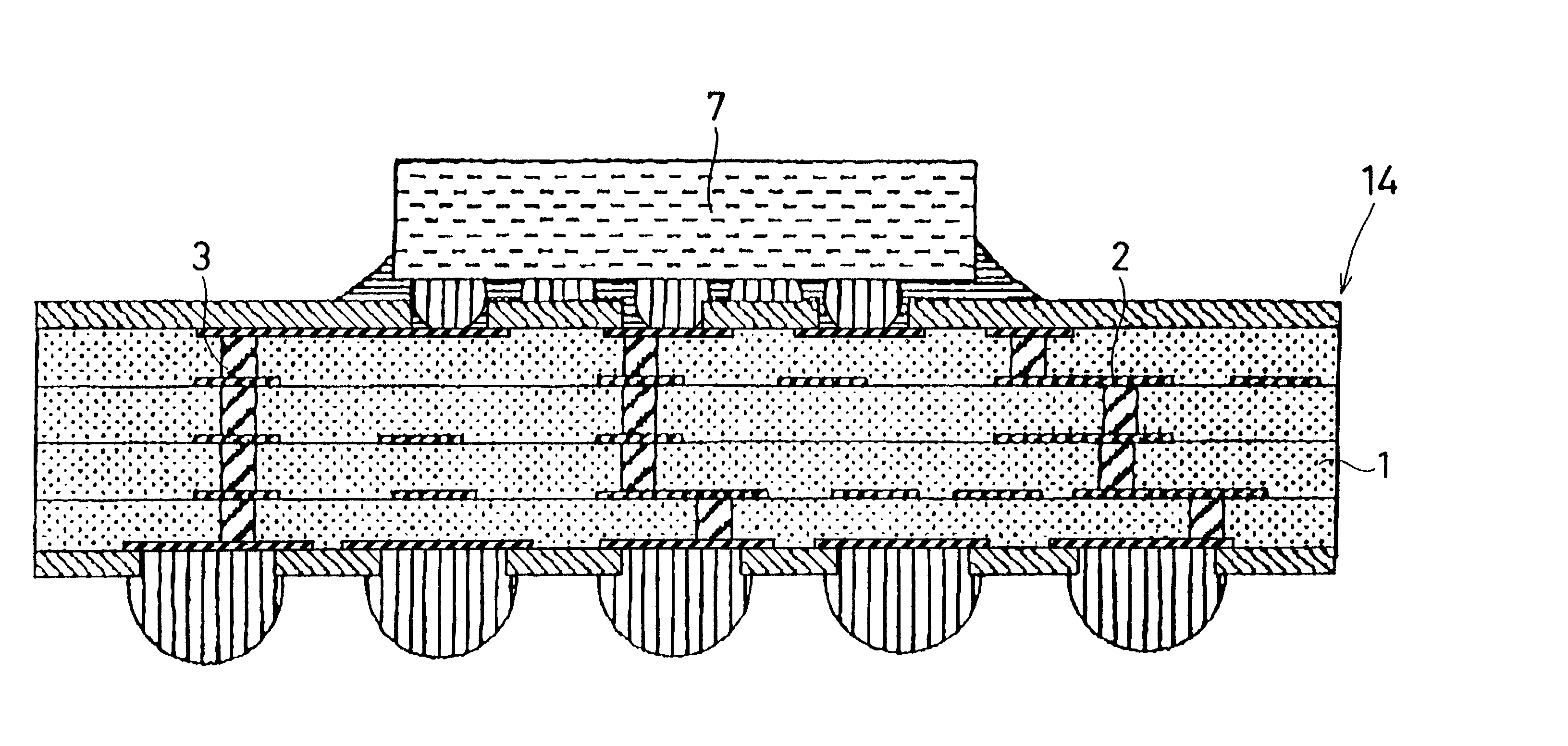
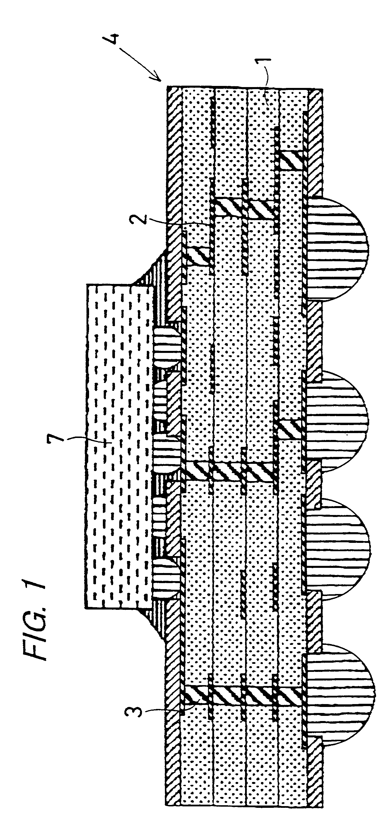
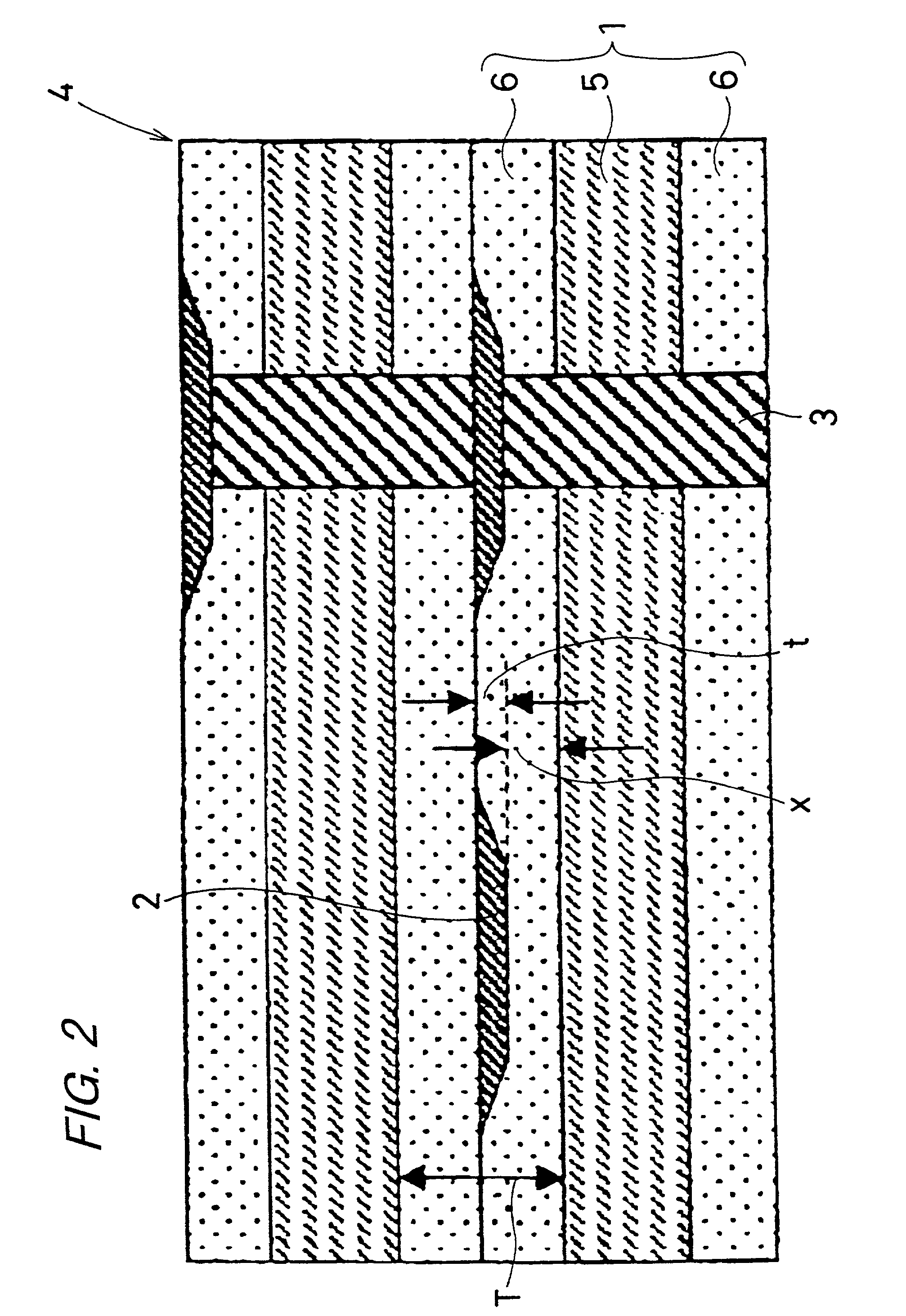
[0144] FIG. 5 is a cross-sectional view of a mixed integrated circuit comprising a semiconductor device mounted on a multi-layer wiring substrate according to a third embodiment of the present invention and FIG. 6 is a enlarged cross-sectional view of a substantial portion of the multi-layer wiring substrate shown in FIG. 5. In this embodiment, parts corresponding to the above-mentioned embodiment are denoted same numerals and explanations with respect to the mare omitted. In these figures, reference numerals 21, 2 and 3 denote a dielectric layer, a wiring conductor and a through conductor, respectively and a multi-layer wiring substrate 24 according to the invention is primarily constructed by these portions. Further, in the present embodiment, the multi-layer wiring substrate 24 comprising 4 layers of the dielectric layers 21 laminated with one another is shown for an illustrative purpose only and by no means for limiting it.

[0145] The dielectric layer 21, which comprises a liquid...


PUM

PropertyMeasurementUnit
Young's modulusaaaaaaaaaa
contact angleaaaaaaaaaa

Abstract

An object of the invention is to satisfy all of a high-density wiring package, soldering thermal resistance, an insulating property and high-frequency transmission characteristics. The invention is a multi-layer wiring substrate having a lamination of a plurality of dielectric layers which are each provided with a wiring conductor made of a metallic foil on at least one of upper and bottom surfaces of the dielectric layer, the wiring conductors between which the dielectric layer is disposed being electrically connected with each other via a through conductor formed in the dielectric layer; on this occasion, the dielectric layers each individually are composed of a liquid crystal polymer layer and cladding layers made of a polyphenyleneether-type organic substance and formed on upper and bottom surfaces of the liquid crystal polymer layer.

Description

[0001] 1. Field of the Invention[0002] The present invention relates to multi-layer wiring substrates for use in electronic instruments such as various types of AV instruments, home electric appliances, communication instruments, computers and peripheral instruments thereof and, particularly, to a multi-layer wiring substrate in which a liquid crystal polymer layer is used as a portion of a dielectric layer.[0003] 2. Description of Related Art[0004] Heretofore, a multi-layer wiring substrate for forming a mixed integrated circuit in which a predetermined electronic circuit is constructed by mounting thereon a multiple of active components such as a semiconductor element and the like, and passive components such as a capacitor element, a resistor element and the like have been formed by forming a vertical through-hole by means of a drill on a dielectric layer made up by impregnating an epoxy resin in glass cloth, forming a plurality of wiring conductors on an inside of the thus-forme...

Claims


Application Information

Patent Timeline
Patent Type & Authority Applications(United States)
IPC IPC(8): H01L23/498H05K1/02H05K1/03H05K3/20H05K3/40H05K3/46
CPCH01L23/49894H01L24/17H01L2924/0102H01L2924/01079H01L2924/15311H05K1/024H05K1/036H05K3/20H05K3/4069H05K3/4614H05K3/4632H05K2201/0141H05K2201/0209H05K2201/068H01L2224/16237Y10T428/24917Y10T428/25Y10T428/24975H01L2224/73204H01L2224/32225H01L2224/16225Y10S428/901H01L2924/01019H01L2924/00012H01L2924/00H01L2924/00014H01L2924/12042H01L2924/14Y10T428/31547Y10T428/31696Y10T428/31909H01L2224/0401
Inventor SERI, TAKUJIHAYASHI, KATSURANAGASAWA, TADASHIKUME, KENJIMATSUNAGA, TAKAHIROMIYATANI, ISAO
Owner KYOCERA CORP
Why Eureka
Try Eureka