Sc-2 based pre-thermal treatment wafer cleaning process

Inactive Publication Date: 2002-12-19
INTERSIL CORP
View PDF3 Cites 26 Cited by
  • Summary
  • Abstract
  • Description
  • Claims
  • Application Information

AI Technical Summary

Problems solved by technology

Unfortunately, a number of limitations associated with conventional processes for growing hydrophilic surface layers of silicon oxide have made it impractical to grow such a silicon oxide layer at a surface concentration of less than 1.times.10.sup.11 atoms/cm.sup.2 of contaminant metals (minority carrier recombination lifetime killers).
Unfortunately, stripping such oxide layers prior to thermal processing is not without its disadvantages, as silicon wafers that have hydrophobic surface layer can be prone to localized (metal) contamination.
Now although the patentee states that the concentration of contaminant metals on the surface of

Method used


Image

  • Sc-2 based pre-thermal treatment wafer cleaning process
  • Sc-2 based pre-thermal treatment wafer cleaning process

Examples


Embodiment Construction

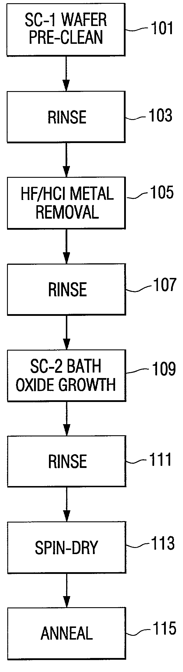
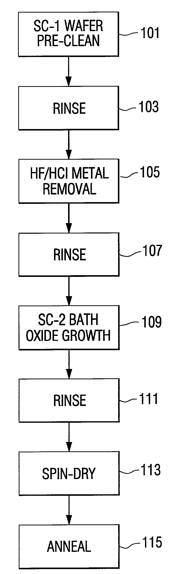
[0025] A cleaning process was carried out on smooth P-type silicon wafers having a resistivity of 5-20 ohm-cm, using a conventional wet bench cleaning apparatus. The cleaning sequence for one set of the wafers (set "A") was as follows:

[0026] STEP 1: 10 minutes in an SC-1 bath (1:1:5 NH.sub.4O:H.sub.2O.sub.2:-H.sub.2O) with megasonics at 50.degree. C.;

[0027] STEP 2: Ultra pure water rinse for 5 minutes;

[0028] STEP 3: 1 minute in a metallic-containing oxide removal solution (5:2:200 HF:HCl:H.sub.2O);

[0029] STEP 4: Overflow deionized water rinse for 5 minutes;

[0030] STEP 5: Immersion in an SC-2 bath (1:1:5 HCl:H.sub.2O.sub.2:H.sub.2-O) for 5 minutes;

[0031] STEP 6: Ultra pure water ines for 5 minutes;

[0032] STEP 7: Spin dried for 10 minutes; and

[0033] STEP 8: Processed through a diffusion furnace (600.degree. C. for 60 minutes) in a nitrogen atmosphere.

[0034] A second set of wafers (set "B") was subjected to steps 1-2 and 5-8.

[0035] The wafers of sets A and B were analyzed for minority ...


PUM

PropertyMeasurementUnit
Timeaaaaaaaaaa
Angleaaaaaaaaaa
Diffusion lengthaaaaaaaaaa

Abstract

Pre heat-treatment processing of a silicon wafer to grow a hydrophilic oxide layer includes an initial step of contacting the wafer with a pre-clean SC-1 bath, thereby producing a silicon wafer surface that is highly particle free. After a deionized water rinse, the wafer is scoured with an aqueous solution containing hydrofluoric acid and hydrochloric acid to remove metallic-containing oxide from the wafer surface. In order to grow a hydrophilic oxide layer, an SC-2 bath (containing hydrogen peroxide and a dilute concentration of metal-scouring HCl) is used. The resulting hydrophilic silicon oxide layer grown on the surface of the silicon wafer using the combined SC-1->AF/HCL->SC-2 wafer cleaning process has a metal concentration no greater than 1x10⁹. The diffusion length of minority carriers is increased from a range on the order of 500-600 microns to a range on the order of 800-900 microns.

Description

[0001] The present invention relates in general to the manufacture of semiconductors, and is particularly directed to a new and improved process for cleaning silicon wafers prior to a heat treatment, so as to minimize the presence of particulates, organics and metallic contaminants that impact minority carrier recombination lifetimes. BACKGROUND[0002] The production of single crystal silicon wafers customarily involves growing a single crystal ingot, slicing the ingot into wafers, and then lapping, etching and polishing the wafers. Based upon the required specifications of a circuit device manufacturer, the silicon wafers may also be subjected to thermal processing, such as, but not limited to, oxygen donor annihilation annealing, thermal processing to control oxygen precipitation, low temperature chemical vapor deposition (CVD) oxidation, epitaxial deposition, and polysilicon deposition.[0003] In the course of such thermal processing, a silicon wafer will typically be exposed to a ...

Claims


Application Information

Patent Timeline
IPC IPC(8): H01L21/304H01L21/306H01L21/316
CPCH01L21/02052H01L21/31662H01L21/02307H01L21/02238H01L21/304
Inventor LINN, JACK H.ROUSE, GEORGE V.RAFIE, SANANOLAN-LOBMEYER, ROBERTA R.HACKENBERG, DIANA LYNNSLASOR, STEVEN T.VALADE, TIMOTHY A.
Owner INTERSIL CORP
Why Eureka
Try Eureka