Catadioptric imaging system and a projection exposure apparatus provided with said imaging system

a technology of imaging system and exposure apparatus, which is applied in the direction of microlithography exposure apparatus, photomechanical treatment, instruments, etc., can solve the problems of increasing light absorption, chromatic aberration becomes impossible, and the practicability of glass materials is limited

Inactive Publication Date: 2003-02-13
NIKON CORP
View PDF0 Cites 22 Cited by
  • Summary
  • Abstract
  • Description
  • Claims
  • Application Information

AI Technical Summary

Benefits of technology

[0023] In the above catadioptric imaging system, the primary image of the first plane (the object plane), that is, an intermediate image, is formed through the first imaging optical system. Then, in the vicinity of the forming position of the intermediate image, there is provided the primary mirror having the front surface reflecting surface in a concave form and having the first radiation transmitting portion (the central opening) at the center thereof, and the diameter of this central opening of this primary mirror is suppressed to reduce the central shielding rate, thereby avoiding deterioration of the image forming performance. Further, such arrangement is employed in which in the vicinity of the second plane (the image plane), there are provided the secondary mirror with a reflecting surface having the second radiation transmitting portion (the central opening) at the center thereof and the lens component adjacently to the secondary mirror on its primary mirror side, so that the central opening of this secondary mirror can be approximated to the second plane. Thus, the central shielding rate is reduced to avoid the deterioration of the image forming performance.
[0114] A method of manufacturing a device by using the above projection exposure apparatus comprises the step of preparing the photosensitive substrate by applying a photosensitive material on the substrate, the step of forming the final image of the mask on the photosensitive substrate through the catadioptric imaging system, the step of developing the photosensitive material on the substrate, and the step of forming a pattern corresponding to the developed photosensitive material on the substrate. According to this device manufacturing method, it is possible to provide an electric device of high density and high precision comprising an extremely fine pattern.

Problems solved by technology

However, if the wavelength of the illumination radiation is reduced, light absorption increases and the kinds of practicable glass materials are limited.
For this reason, in a projection optical system which is constituted only by a refractive lens system, or only by lens components containing no reflecting mirror with a refracting power (a concave reflecting mirror or a convex reflecting mirror), it becomes impossible to correct a chromatic aberration.
However, in order to achieve a desired optical performance in a dioptric projection system, a large number of lens components is required, so that it is inevitable to reduce the transmittance or to increase the production cost.
However, since the optical path separation methods disclosed in Japanese Patent Publication No.
As a result, it is inevitable to increase the cost for producing the optical system.
As a result, due to this central shielding of the imaging beams, the image forming characteristic of the optical system is degraded.
However, when this optical system is applied to a projection optical system which uses exposure light having the wavelength of 180 nm or less, materials usable for forming a half-transmitting thin film are limited, so that it is difficult to produce a half mirror having a satisfactory performance.
Also, only not more than a fourth of the light quantity reaches the wafer plane, so that the throughput is inevitably lowered.
However, these disclosed optical systems have the drawbacks as described below.
Further, it is also impossible to largely reduce a WD on the image side (a working distance which is an axial air space between the lens surface which is closest to a wafer and the wafer in the projection optical system) on the image side, taking into account an influence of a gas out from a resist (which is coated on the wafer) at the time of exposure and an influence of a drive of a wafer stage.
As a result, not only the production of such optical system becomes difficult, the manufacturing cost increases drastically.
However, when such optical system is applied to a projection optical system in which a reduction rate of 0.15 to 0.4 or around is required for the entire system, the refracting power of the first imaging optical system inevitably increases, and the chromatic aberration in the first imaging optical system generated in the first imaging optical system also inevitably increases.
As a result, in this optical system, it is difficult to correct the chromatic aberration satisfactorily while maintaining particularly the diameters and the thickness of the two reflecting mirrors to be practicable.
However, in this optical system, like in the optical system disclosed in U.S. Pat. No. 5,488,299, a concave mirror which is provided in the vicinity of the forming position of an intermediate image is a rear surface reflecting mirror for the purpose of correcting the chromatic aberration, so that the diameter of the concave mirror becomes conspicuously large and not practicable to achieve an image circle having a predetermined size on the image side.
However, when a fluorite lens with a rear surface reflecting coat applied thereon is used, the following drawbacks may be generated.
That is, film material for the coat for reflecting light in such wavelength range are limited and light absorption thereof is comparatively large.
As a result, such tendency is liable to occur that the lens surface shape of fluorite having a large coefficient of thermal expansion varies during exposure so as to deteriorate the image forming performance.
On the other hand, below the lower limit of the conditional expression (1), it becomes unfavorably impossible to correct the chromatic aberration with excellency while maintaining the secondary mirror to be in a realizable size.
Incidentally, when the wavelength of the exposure light becomes 180 nm or lower, film materials for the antireflection coat to be applied on the surface of the lens component are limited, and a sufficient performance can not be obtained as the antireflection coat.
However, this arrangement does not prevent a plane parallel plate or the like from being provided in an optical path between the secondary mirror and the second plane.
Above the upper limit of the conditional expression (2), the aberrations generated in the second imaging optical system become larger, and excellent correction particularly of a spherical aberration, a coma, and a chromatic aberration becomes unfavorably difficult.
On the other hand, below the lower limit of the conditional expression (2), the aberrations generated in the first imaging optical system become larger, so that the entire system is inevitably and unfavorably enlarged.
Above the upper limit of the conditional expression (3), a deviation in the curvature of field for each wavelength becomes larger, so that it becomes impossible to conduct excellent chromatic aberration correction.
A high-order aberration, such as a chromatic coma, is also unfavorably generated.
Conversely, below the lower limit of the conditional expression (3), the first-order chromatic aberration is not sufficiently corrected unfavorably.
Above the upper limit of the conditional expression (4), aberrations generated in the second imaging optical system become larger, and excellent correction of a spherical aberration, a coma, and a chromatic aberration, particularly, becomes unfavorably difficult.
On the other hand, below the lower limit of the conditional expression (4), aberrations generated in the first imaging optical system become larger, so that the entire system is inevitably and unfavorably enlarged.
Here, when the variable aperture stop and the central shielding member are disposed at the same position, not only that a mechanical interference is brought about between the variable aperture stop and the central shielding member, but also a difference in the numerical apertures is unfavorably generated due to a difference in the image height (the object-height) when the aperture size of the variable aperture stop is changed.
However, in this case, the catadioptric imaging system becomes unfavorably complicated with, for example, the enlarged total length or the increased number of the lenses.
Below the lower limit of the conditional expression (5), the power of the chromatic aberration correction negative lens becomes smaller so that it is difficult to realize excellent chromatic aberration correction.
Conversely, above the upper limit of the conditional expression (5), another aberration may be generated so that it is difficult to produce the chromatic aberration correction negative lens itself.
That is, when an exposure wavelength becomes 180 nm or less, the film materials used for an antireflection coat which is applied on the surfaces of the refracting lenses are limited, so as not to obtain a sufficient performance as the antireflection coat.
As a result, an excellent image forming performance can not be obtained.
On the other hand, above the upper limit of the conditional expression (8), the central shielding becomes large so that an optical system having a sufficiently excellent image forming performance can not be achieved.
For this reason, in case of detecting the position of the second plane, it is difficult to conduct the focal detection by the conventional oblique incidence method.

Method used


Image

  • Catadioptric imaging system and a projection exposure apparatus provided with said imaging system
  • Catadioptric imaging system and a projection exposure apparatus provided with said imaging system
  • Catadioptric imaging system and a projection exposure apparatus provided with said imaging system

Examples


second example

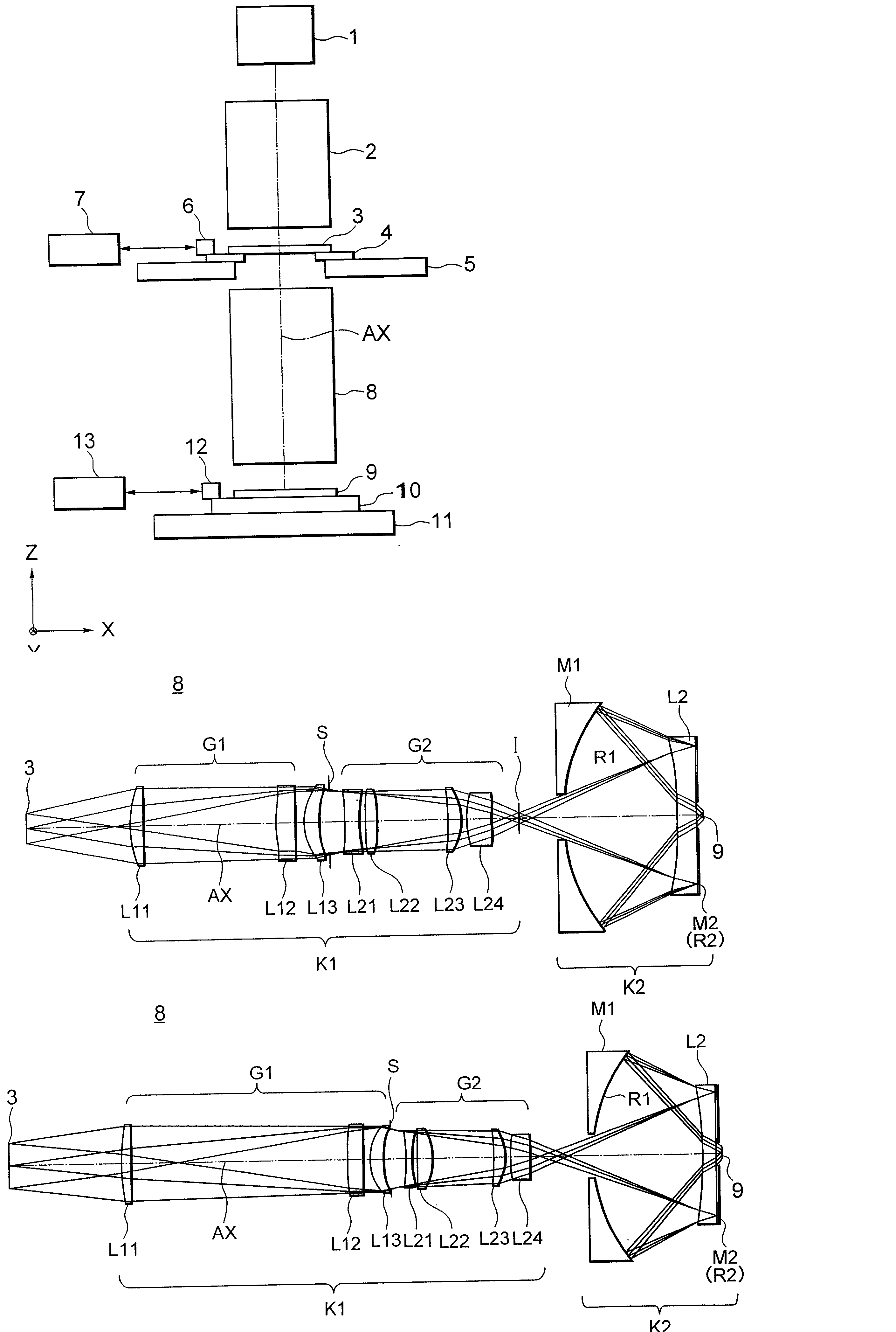
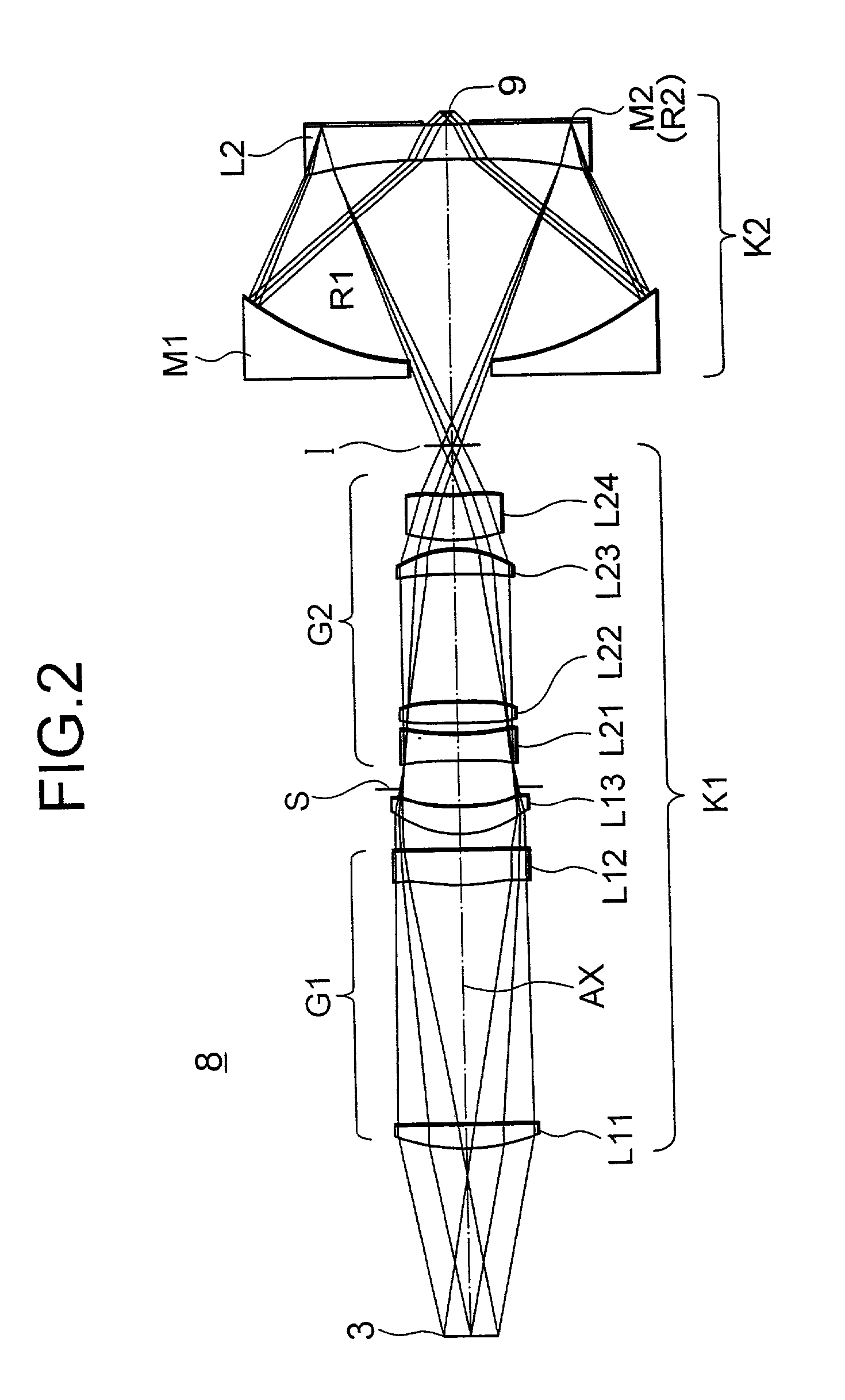
[0172] FIG. 4 is a view for showing a lens structure of a catadioptric imaging system (projection optical system) according to a second example. In the second example, like in the first example, the present invention is applied to a projection optical system in which the aberrations including the chromatic aberration are corrected for the exposure light having the wavelength width of 157.6 nm.+-.10 pm.

[0173] In the catadioptric imaging system of FIG. 4, the first lens group G1 is comprised of a double convex lens L11 having the surface on the mask side formed to be aspherical, a positive meniscus lens L12 having the aspherical convex surface facing the mask side, and a positive meniscus lens 13 having the aspherical concave surface facing the wafer side, in this order from the mask side.

[0174] Also, the second lens group G2 is comprised of a double concave lens L21 having the surface on the mask side formed to be aspherical, a double convex lens L22 having the surface on the mask si...

third example

[0183] FIG. 6 is a view for showing a lens structure of a catadioptric imaging system (projection optical system) according to a third example. In the third example, unlike in the first and second examples, the present invention is applied to a projection optical system in which the aberrations including the chromatic aberration are corrected for the exposure light having the wavelength width of 157.6 nm.+-.2 pm.

[0184] In the catadioptric imaging system of FIG. 6, the first lens group G1 is comprised of a double convex lens L11 having the surface on the mask side formed to be aspherical, a double convex lens L12 having the surface on the mask side formed to be aspherical, and a positive meniscus lens 13 having the aspherical concave surface facing the wafer side, in this order from the mask side.

[0185] Also, the second lens group G2 is comprised of a double concave lens L21 having the surface on the mask side formed to be aspherical, a double convex lens L22 having the surface on th...

fourth example

[0194] FIG. 8 is a view for showing a lens structure of a catadioptric imaging system (projection optical system) according to a fourth example. In the fourth example, like in the third example, the present invention is applied to a projection optical system in which the aberrations including the chromatic aberration are corrected for the exposure light having the wavelength width of 157.6 nm.+-.2 pm.

[0195] In the catadioptric imaging system of FIG. 8, the first lens group G1 is comprised of a positive meniscus lens L11 having the aspherical concave surface facing the mask side, a positive meniscus lens L12 having the aspherical convex surface facing the mask side, a negative meniscus lens L13 having the aspherical concave surface facing the mask side, and a positive meniscus lens L14 having the aspherical convex surface facing the mask side, in this order from the mask side.

[0196] Also, the second lens group G2 is comprised of a negative meniscus lens L21 having the aspherical conc...


PUM

PropertyMeasurementUnit
diameteraaaaaaaaaa
wavelengthaaaaaaaaaa

Abstract

The object of the present invention is to provide a catadioptric imaging system, or the like, which is capable of obtaining a desired image-side NA and an image circle without increasing the size of a reflecting mirror with a smaller number of lenses. This catadioptric imaging system comprises a first imaging optical system and a second imaging optical system, wherein the first imaging optical system is provided with a positive first lens group, an aperture stop, and a positive second lens group in the order from the object side, and the second imaging optical system is provided with a primary mirror comprising a concave first reflecting surface having a first radiation transmitting portion at the center thereof, and a secondary mirror comprising a second reflecting surface having a second radiation transmitting portion at the center thereof. In this case, all of the refracting members for constituting the optical system is formed of the same optical material, or at least one of the refracting surfaces and the reflecting surfaces is formed to be aspherical, or a refracting member is disposed to be separated from the first reflecting surface or the second reflecting surface.

Description

[0001] This application claims the benefit of International application PCT / JP99 / 07225 and Japanese Patent application Nos. 10-370143 and 11-066769 which are hereby incorporated by reference.[0002] The present invention relates to a catadioptric imaging system which is preferably used in projection exposure for producing, for example, a semiconductor device, a liquid crystal display device, or the like, by photolithography, as well as a projection exposure apparatus and an exposure method using such catadioptric imaging system, and more particularly, to a catadioptric imaging system, or the like, which attains a resolution of 0.1 .mu.m or lower in the ultraviolet region by using a reflection system as a factor of an imaging optical system inside a catadioptric imaging system.BRIEF DESCRIPTION OF THE PRIOR ART[0003] In a process of photolithography for producing a semiconductor device, or the like, there is employed a projection exposure apparatus which performs projection exposure o...

Claims


Application Information

Patent Timeline
Patent Type & Authority Applications(United States)
IPC IPC(8): G02B17/08G03F7/20
CPCG02B17/0808G02B17/0812G02B17/0856G02B17/0892G03F7/70225G02B3/04
Inventor OMURA, YASUHIRO
Owner NIKON CORP
Why Eureka
Try Eureka