Aggregate of Semicnductor micro-needles and method of manufacturing the same, and semiconductor apparatus and method of manufacturing the same

a technology of semi-cnductors and micro-needles, which is applied in the manufacture of final products, sustainable manufacturing/processing, instruments, etc., can solve the problems of difficult control of the diameter and depth of the micro-pore 102 formed by anodization, difficult to achieve the effect of enhancing the quantum size effect and facilitating manufacturing

Inactive Publication Date: 2003-03-27
PANASONIC CORP
View PDF0 Cites 11 Cited by
  • Summary
  • Abstract
  • Description
  • Claims
  • Application Information

AI Technical Summary

Benefits of technology

0037] In accordance with the method, a semiconductor apparatus with the advanced information processing function as described above can easily be manufactured.
0038] It is possible to further provide the step of forming a p-n junction in the above silicon substrate and form, in the above step ...

Problems solved by technology

That is, in a normal semiconductor apparatus composed of single-crystal silicon, an excited electron makes an indirect transition to a lower energy level so that the energy resulting from the transition is converted into heat, which renders light emission in the visible region difficult.
However, if electroluminescence is to be obtained by the application of an electric field or photoluminescence is to be obtained by the irradiation with light of the porous silicon formed by anodization in the surface region of the silicon substrate 101 as shown in FIG. 33, the following problems are encountered.
That is, the diameter and depth of the micro-pore 102 formed by anodization are difficult to control.
In addition, the configuration of the micro-pore 102 is complicated and the distribution of its wall thickness is extremely random.
As a result, if etching is intensely performed in order to reduce the wall thickness, the wall portions may be partially torn and peeled off the substrate.
Moreover, since the distribution of the wall thickness is random, the quantum size effects a...

Method used


Image

  • Aggregate of Semicnductor micro-needles and method of manufacturing the same, and semiconductor apparatus and method of manufacturing the same
  • Aggregate of Semicnductor micro-needles and method of manufacturing the same, and semiconductor apparatus and method of manufacturing the same
  • Aggregate of Semicnductor micro-needles and method of manufacturing the same, and semiconductor apparatus and method of manufacturing the same

Examples


first embodiment

[0075] (First Embodiment)

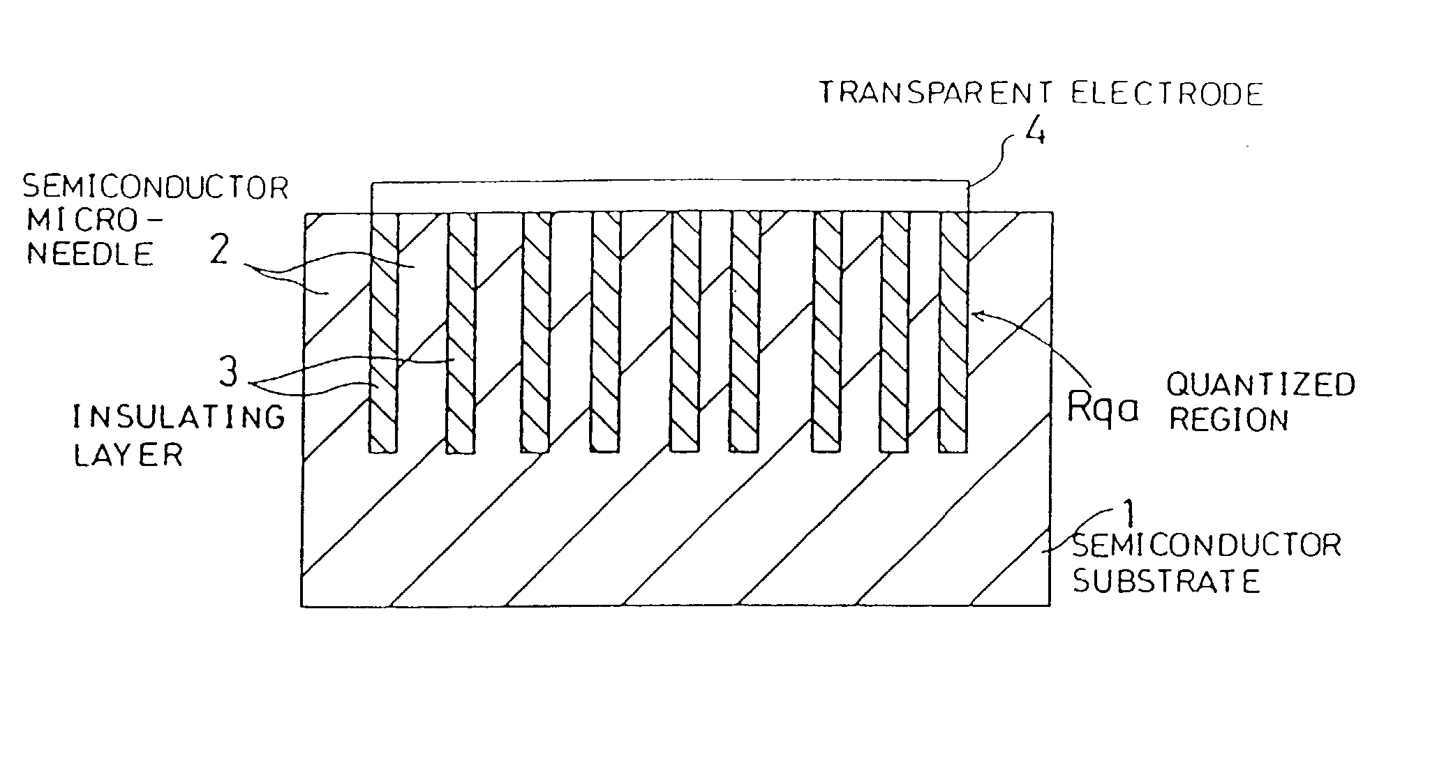
[0076] A description will be given first to a first embodiment. FIG. 1 is a cross-sectional view of an optical semiconductor apparatus according to the first embodiment. As shown in the drawing, the semiconductor apparatus comprises: a silicon substrate 1 of single-crystal structure; a large number of semiconductor micro-needles 2 extending from the surface of the silicon substrate 1 to a specified depth so that the axial direction thereof is perpendicular to the surface of the substrate 1; an insulating layer 3 composed of a silicon dioxide film which fills up the space surrounding each semiconductor micro-needle 2; and a transparent electrode 4 formed on the flattened top ends of the semiconductor micro-needles 2 and the insulating layer 3. An aggregate of the foregoing semiconductor micro-needles 2 functions as a quantized region Rqa. Those ends of the above semiconductor micro-needles 2 which are closer to the substrate 1, hereinafter referred to as "bas...

second embodiment

[0107] (Second Embodiment)

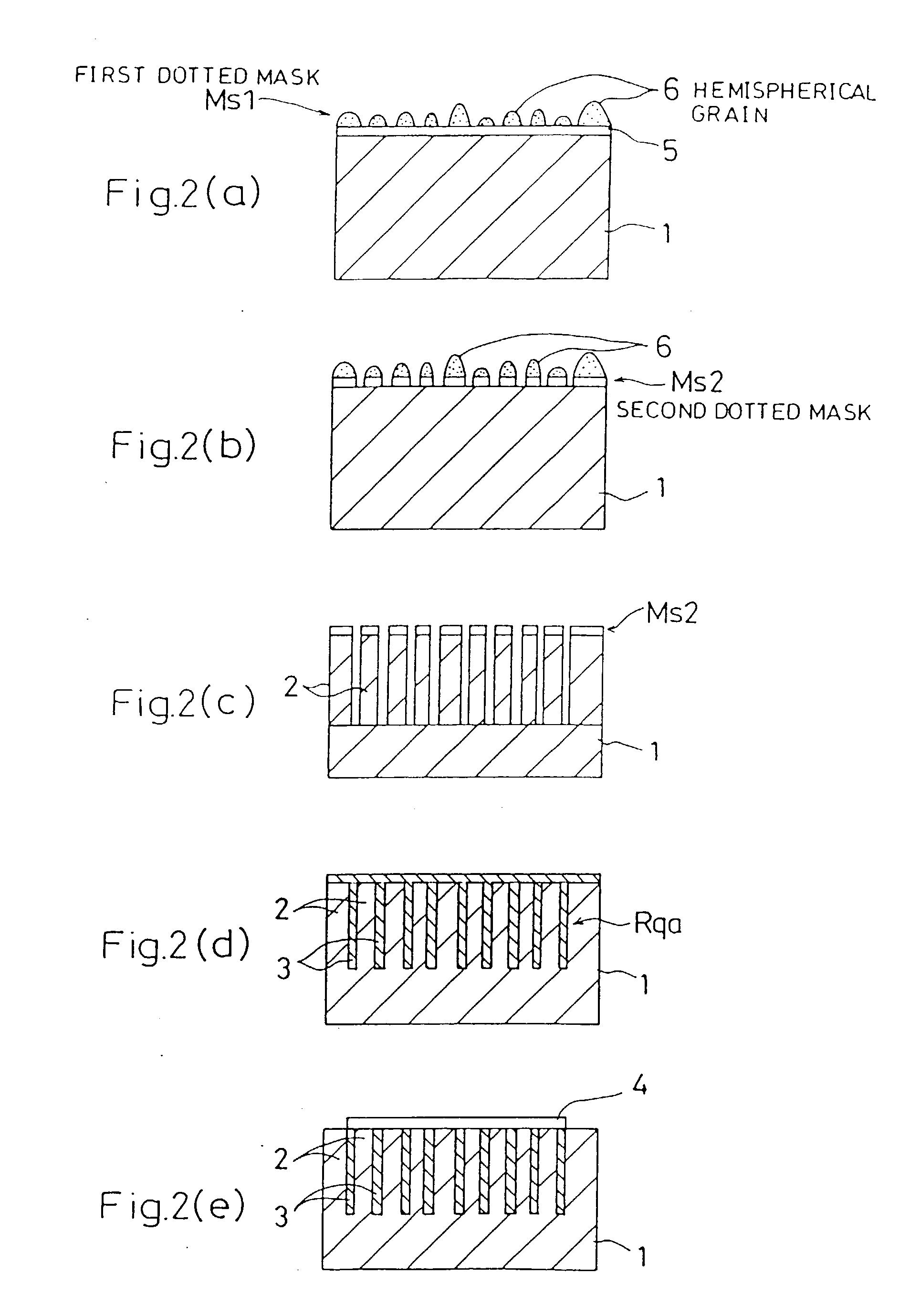
[0108] Next, a description will be given to a second embodiment. FIGS. 8(a) to 8(e) illustrate the process of manufacturing the optical semiconductor apparatus according to the second embodiment. The manufacturing process used in the second embodiment is substantially the same as the manufacturing process used in the above first embodiment, except that the conditions under which the hemispherical grains 6 are deposited by LPCVD are changed and that the space surrounding each semiconductor micro-needle 2 is filled up with a silicon dioxide film 3b formed by CVD or the like after the side portions of the semiconductor micro-needles 2 were covered with a thermal oxidation film 3a, followed by the flattening of their surface regions. In other words, these two types of oxide films 3a and 3b constitute an insulating layer 3.

[0109] In the step of depositing the hemispherical grains 6, a He-based 15% SiH.sub.4 gas is used as a raw material so as to deposit the hemi...

third embodiment

[0117] (Third Embodiment)

[0118] Next, a description will be given to a third embodiment for improving the configuration of the hemispherical grain 6. After the hemispherical grains 6 are formed by substantially the same manufacturing process as that of the above first embodiment, the SiH.sub.4 gas in a tube is evacuated, followed by annealing while introducing N.sub.2 gas, which is an inactive gas, into the tube. FIG. 11 shows the relationship between the annealing period and the grain diameter and density. It will be appreciated that the grain diameter decreases with an increase in annealing period. Since the surface and interface tend to shrink with a decrease in grain diameter, the configuration of the grain becomes closer to a hemisphere, resulting in a high increase rate of the surface area of the grain. If the annealing period becomes 2 minutes or longer, the region with no hemispherical grain expands. The increasing difficulty with which the hemispherical grains 6 are formed ...


PUM


Abstract

On a silicon substrate is formed a silicon dioxide film and then hemispherical grains made of silicon, each having an extremely small diameter, are deposited thereon by LPCVD. After annealing the hemispherical grains, the silicon dioxide film is etched using the hemispherical grains as a first dotted mask, thereby forming a second dotted mask composed of the silicon dioxide film. The resulting second dotted mask is used to etch the silicon substrate to a specified depth from the surface thereof, thereby forming an aggregate of semiconductor micro-needles. Since the diameter of each of the semiconductor micro-needles is sufficiently small to cause the quantum size effects as well as has only small size variations, remarkable quantum size effects can be obtained. Therefore, it becomes possible to constitute a semiconductor apparatus with a high information-processing function by using the aggregate of semiconductor micro-needles (quantized region).

Description

BACKGROUND OF THE INVENTION[0001] In recent years, there has been developed an optical element in which porous silicon is formed to be used as a light emitting element. Japanese Laid-Open Patent Publication No. 4-356977 discloses such an optical element, in which a large number of micro-pores 102 are formed in the surface region of a silicon substrate 101 by anodization, as shown in FIG. 33. If the porous silicon is irradiated with light, photo-luminescence having its absorption edge in the visible region is observed, which implements a light-receiving / light-emitting element using silicon. That is, in a normal semiconductor apparatus composed of single-crystal silicon, an excited electron makes an indirect transition to a lower energy level so that the energy resulting from the transition is converted into heat, which renders light emission in the visible region difficult. However, there has been reported a phenomenon that, if silicon has a walled structure, such as porous silicon, ...

Claims


Application Information

Patent Timeline
IPC IPC(8): B81B3/00G01Q60/38G02B6/12G02B6/124G10H1/00G10H7/02G11C23/00H01H1/00H01L21/308H01L31/0352H01L31/18H01L33/18H01L33/20
CPCB82Y10/00Y02E10/547G02B2006/12102G02B2006/12173G02B2006/12176G10H1/0041G10H7/02G11C23/00H01H1/0036H01L21/3086H01L31/0352H01L31/1804H01L33/08H01L33/18H01L33/20G02B6/1245Y02P70/50
Inventor ERIGUCHI, KOJIKUBOTA, MASAFUMINIWA, MASAAKINOMURA, NOBORU
Owner PANASONIC CORP
Why Eureka
Try Eureka