Semiconductor light emission element, semiconductor composite element and process for producing semiconductor light emission element

a technology of semiconductor light emission element and semiconductor composite element, which is applied in the direction of semiconductor devices, basic electric elements, electrical apparatus, etc., can solve the problems of accelerating junction defects, inability to grow crystals of high quality, and inability to emit ligh

Inactive Publication Date: 2003-09-25
FUJIFILM BUSINESS INNOVATION CORP
View PDF3 Cites 18 Cited by
  • Summary
  • Abstract
  • Description
  • Claims
  • Application Information

AI Technical Summary

Problems solved by technology

However, silicon cannot emit light as it is because it is an indirect transition semiconductor.
Therefore, direct transition III-V compound semiconductors (nitride semiconductors), which emit light, are formed on silicon, but it is the current situation that there is a problem in that crystals of high quality cannot be grown.
Particularly, in the case where there is a large difference in thermal expansion coefficient between the two semiconductors, it is considered that large stress is formed after cooling because a high temperature is applied upon forming the nitride semiconductor, whereby not only the formation of junction defects is accelerated, but also structural defects, such as cracking, crazing and interfacial exfoliation, are caused.
However, two-step growth is carried out for growing the nitride semiconductor by using a buffer layer formed with GaN, AlN or ZnO, and therefore, the semiconductor substrate formed with the dissimilar semiconductor, such as Si and GaAs, functions only as a substrate to grow the nitride semiconductors but does not serve as a semiconductor light emission element.
Furthermore, there are such problems that the nitride semiconductor crystals are formed by providing a buffer layer, such as GaN, AlN and ZnO, at the interface to the dissimilar semiconductor, and the semiconductor junction cannot be directly formed.
As described in the foregoing, in the semiconductor light emission element having a constitution containing a nitride semiconductor layer and a dissimilar semiconductor (semiconductor substrate) different therefrom, the nitride semiconductor layer and the dissimilar semiconductor (semiconductor substrate) are formed through the buffer layer, such as GaN, AlN and ZnO, having insulating property, and the dissimilar semiconductor does not contribute to injection of charge (electrons or positive holes), whereby a large number of layers are required, and problems in cost are caused.
As a result, there are problems of complex layer s

Method used


Image

  • Semiconductor light emission element, semiconductor composite element and process for producing semiconductor light emission element
  • Semiconductor light emission element, semiconductor composite element and process for producing semiconductor light emission element
  • Semiconductor light emission element, semiconductor composite element and process for producing semiconductor light emission element

Examples


example 1

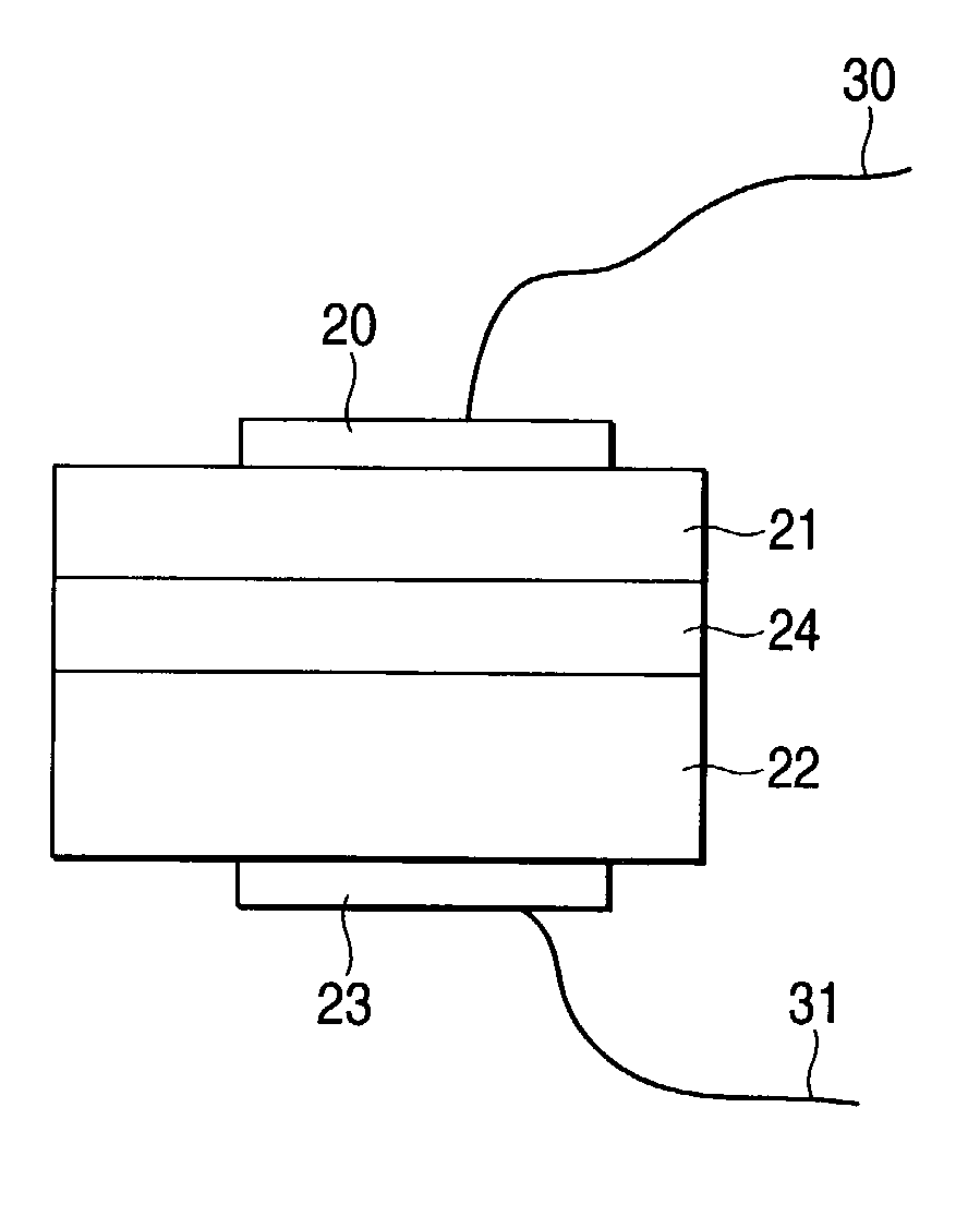
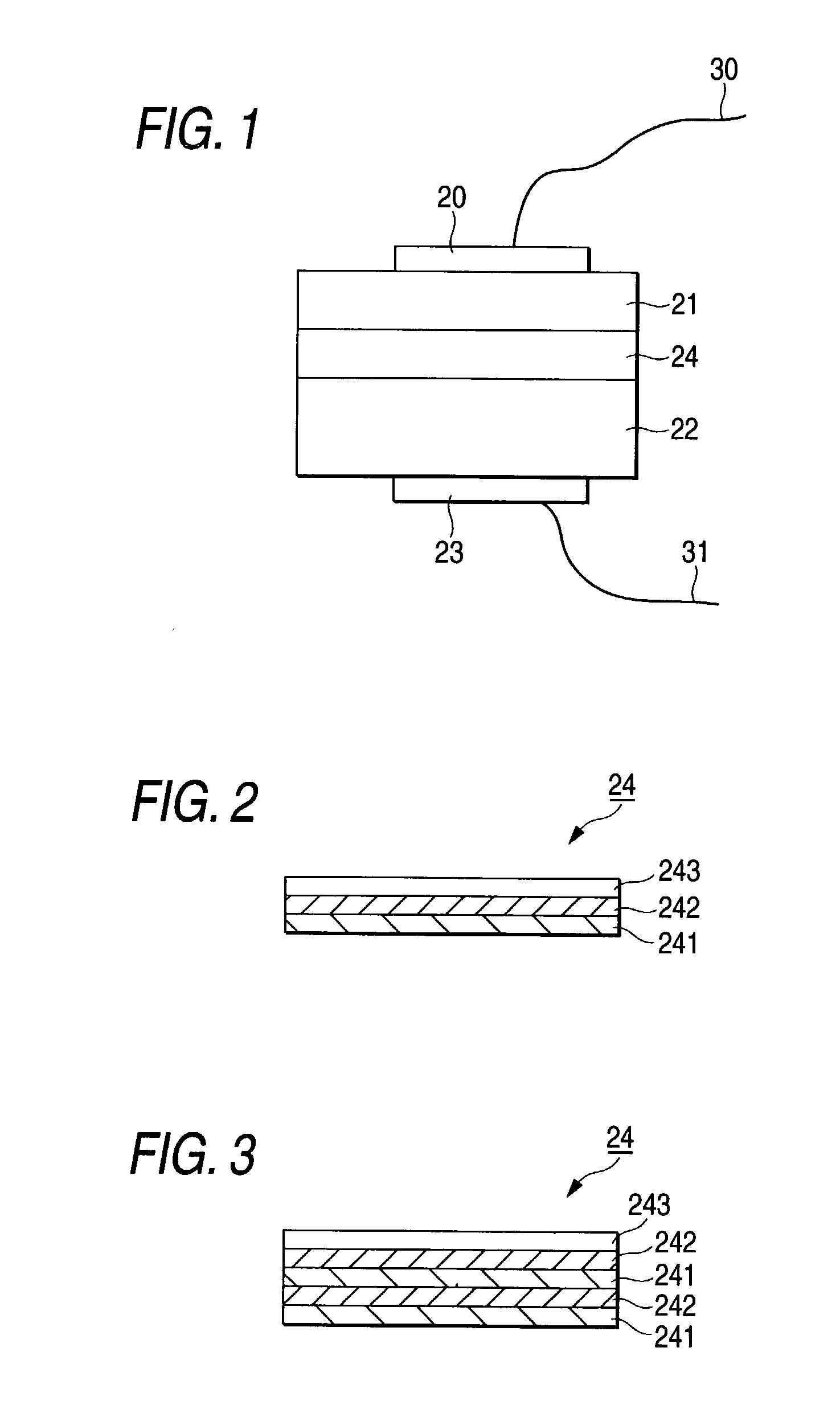
[0089] Formation of Light Emission Layer

[0090] Au is vapor-deposited to a thickness of 0.1 .mu.m to provide an ohmic contact electrode on one surface of a p-type silicon substrate (thickness: 350 .mu.m) having a resistivity of 2 .OMEGA.cm and a plane direction (100), which has been etched with a hydrofluoric acid aqueous solution having a concentration of 10% by weight. The silicon substrate is put on the substrate holder 3 of the layer formation apparatus shown in FIG. 6 in such a manner that the surface opposite to the surface having the electrode thus vapor-deposited faces the gas inlet tubes, and after evacuating the interior of the vessel 1 to vacuum through the exhaust opening 2, the substrate is heated to 300.degree. C. with the heater 4. An N.sub.2 gas is introduced to the quartz tube 5 having a diameter of 25 mm at 2,000 sccm through the gas inlet tube 9, and discharge is carried out through the microwave waveguide tube 8 with a microwave output of 2.45 GHz set at 250 W und...

example 2

[0098] Formation of Light Emission Layer

[0099] The same substrate as in Example 1 is used. Film formation is carried out for 10 minutes under such conditions that hydrogen-diluted silane is introduced at 0.1% by atom from the gas inlet tube 12 to form a GaN:H film (hydrogenated GaN film) doped with a slight amount of Si having a thickness of 100 nm, which is used as a light emission layer, directly on the surface of the silicon substrate.

[0100] Formation of Nitride Semiconductor Layer Contributing to Charge Injection

[0101] Hydrogen-diluted silane is introduced at 1% by atom through the gas inlet tube 12, and under that condition, film formation is carried out for 10 minutes to form an n-type Si-doped GaN:H film (hydrogenated GaN film) having a thickness of 0.1 .mu.m, which is used as the nitride semiconductor layer contributing to charge injection, on the light emission layer.

[0102] The hydrogen composition of the n-type Si-doped GaN:H film measured by HFS (hydrogen forward scatteri...

example 3

[0105] Formation of Light Emission Layer (Fluorescent Inorganic Compound)

[0106] The same substrate as in Example 1 is used. Film formation is carried out for 10 minutes under the conditions of only the trimethyl gallium gas and the nitrogen remote plasma and in a state that the substrate temperature is a room temperature in Example 1 to form a film containing a fluorescent inorganic compound having a thickness of 10 nm, which is used as a light emission layer, directly on the surface of the silicon substrate. The film containing the fluorescent inorganic compound contains about 30% by atom of oxygen and about 10% by atom of carbon, as well as Ga and nitrogen.

[0107] A film formed under the same conditions on the same substrate as in Example 1 for 1 hour is taken out into the air and then irradiated with an ultraviolet ray having a wavelength of 325 nm from a He--Cd laser. The film exhibits strong blue fluorescence.

[0108] Formation of Nitride Semiconductor Layer contributing to Charge...


PUM


Abstract

A simple and low cost semiconductor light emission element exerting high performance and a process for producing the same are provided. The semiconductor light emission element contains a nitride semiconductor layer containing at least one or more element selected from Group IIIA elements and one or more element selected from Group VA element, a dissimilar semiconductor having a polarity different from the nitride semiconductor layer, and a light emission layer provided between the dissimilar semiconductor and the nitride semiconductor, in which electrons or positive holes are injected from semiconductors of the dissimilar semiconductor and the nitride semiconductor layer to the light emission layer to carry out light emission.

Description

[0001] 1. Field of the Invention[0002] The present invention relates to a semiconductor light emission element using a nitride semiconductor, a semiconductor composite element and a process for producing a semiconductor light emission element.[0003] 2. Description of the Related Art[0004] Wide band gap semiconductors have been receiving attention as a semiconductor for a blue light emission element in recent years (S. Nakamura, T. Mukai and M. Senoh, Jpn.J. Appl. Phys., vol. 30, L1998 (1991); and S. Nakamura, M. Senoh, S. Nagahama, N. Iwata, T. Yamada, M. Matsushita, Y. Sugimoto and H. Kiyoku, Appl. Phys. Lett., vol. 69, p. 1477 (1996)). Among them, nitride semiconductors (nitride compound semiconductors) are receiving attention as the wide band gap semiconductor.[0005] However, the nitride semiconductors are often produced by a two-step growth, in which a low temperature buffer layer is firstly formed by using a sapphire substrate, and after increasing the temperature to about 1,00...

Claims


Application Information

Patent Timeline
IPC IPC(8): H01L21/205H01L33/32H01L33/50
CPCH01L33/26H01L33/32H01L33/30
Inventor YAGI, SHIGERU
Owner FUJIFILM BUSINESS INNOVATION CORP
Why Eureka
Try Eureka