
Photoelectric conversion device and manufacturing process thereof

a technology of photoelectric conversion and manufacturing process, which is applied in the direction of semiconductor/solid-state device details, radiation controlled devices, final product manufacturing, etc., can solve the problems of reducing the advantage of using crystalline semiconductor particles, unable to maintain the structure, and difficult to deposit semiconductor particles with less than 0.2 mm particle sizes on the substra

Inactive Publication Date: 2004-01-15
KYOCERA CORP
View PDF2 Cites 36 Cited by
  • Summary
  • Abstract
  • Description
  • Claims
  • Application Information

AI Technical Summary

Benefits of technology

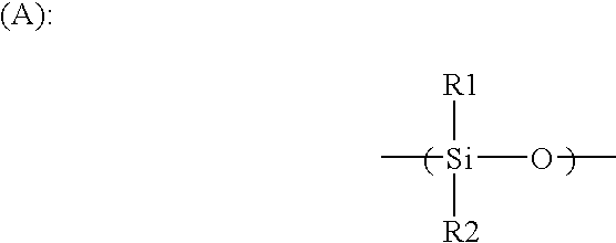
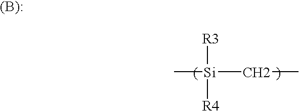
[0009] A photoelectric conversion device according to the present invention comprises a substrate, numerous crystalline semiconductor particles deposited on the substrate and joined thereto via alloy portions melted between the substrate and the crystalline semiconductor particles by application of heat, and an insulator interposed among the numerous crystalline semiconductor particles, in which an organic-inorganic composite comprising a mixture or reaction product of polysiloxane and polycarbosilane is used for the insulator. With this structure, generation of defects such as cracking and peeling in the insulator and crystalline semiconductor particles can be prevented. Accordingly, it is possible to form a stable insulator so as to ensure separation of the positive electrode from the negative electrode. In addition, since this structure allows for lower accuracy of particle diameter, the manufacturing margin can be improved. Accordingly, it is possible to provide a low cost photoelectric conversion device with high reliability.
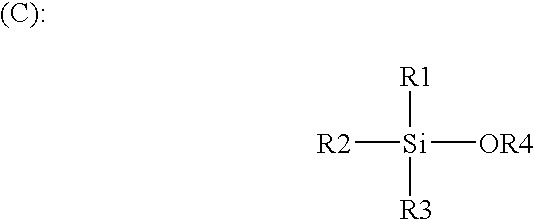
[0011] A photoelectric conversion device according to the present invention comprises a substrate, numerous crystalline semiconductor particles deposited on the substrate and joined thereto via alloy portions melted between the substrate and the crystalline semiconductor particles by application of heat, and an insulator interposed among the numerous crystalline semiconductor particles, in which a mixture comprising an organic-inorganic composite containing Si and a hydrolyzate of alkoxysilane is used for the insulator. With this structure, generation of defects such as cracking and peeling in the insulator and crystalline semiconductor particles can be prevented. Accordingly, it is possible to form a stable insulator so as to ensure separation of the positive electrode from the negative electrode. In addition, since this structure allows for lower accuracy of particle diameter, the manufacturing margin can be improved. Thus, it is possible to manufacture a low cost photoelectric conversion device with high reliability.
[0013] A process of manufacturing a photoelectric conversion device according to the present invention comprises the steps of: depositing numerous crystalline semiconductor particles of one conductivity type on a substrate having an electrode of one side and applying heat thereto so as to join the crystalline semiconductor particles to the substrate; forming a coating having liquid repellency on the crystalline semiconductor particles; applying a solution or liquid dispersion of an insulating material over the crystalline silicon particles and performing a heat treatment so as to interpose the insulating material among the crystalline semiconductor particles; forming a semiconductor layer of the opposite conductivity type over the crystalline semiconductor particles; and connecting an electrode of another side to the semiconductor layer of the opposite conductivity type. By this process, it is possible to selectively form a coating having liquid repellency only on the crystalline semiconductor particles and interpose the insulating material among the crystalline semiconductor particles. Therefore, the thickness of the insulator can be easily controlled, so that generation of defects such as cracking and peeling in the insulator and crystalline semiconductor particles can be prevented. Accordingly, it is possible to ensure separation of the positive electrode from the negative electrode by the insulator. In addition, this process allows for lower accuracy of the particle size, so that the manufacturing margin can be improved. As a result, it is possible to provide a low cost manufacture of photoelectric conversion devices. In addition, since the insulator can be formed without allowing the insulating material to remain on the crystalline semiconductor particles, adequate pn-junction area can be provided. Thus, it is possible to manufacture a photoelectric conversion device having higher conversion efficiency than conventional photoelectric conversion devices.

Problems solved by technology

Using crystalline semiconductor particles with particle sizes exceeding 1.0 mm makes no difference in quantity of silicon from the amount used in conventional crystal plate type photoelectric conversion devices including the amount of ground part, which nullifies the advantage of using crystalline semiconductor particles.
In addition, crystalline semiconductor particles with particle sizes less than 0.2 mm are difficult to be deposited on the substrate 1, which is another problem.
However, in such a case, it is feared that the contact between the substrate 1 and the crystalline semiconductor particles 2 is so weak that the crystalline semiconductor particles leave the substrate, failing to maintain the structure as a solar cell.
Therefore, when the polycarbosilane content is large, cracking is likely to occur, so that it is difficult to form a thick insulator 3.
When it is more than 0.25, another problem arises in that the insulator becomes hard to be filled into the interstices among the crystalline semiconductor particles 2, so that the insulation performance deteriorates.
On the other hand, when the average particle size is more than 10 .mu.m, the formability deteriorates, causing the problem of insulation failure.
For this reason, light beams that are not directly incident on the crystalline semiconductor particles cannot be utilized effectively, and as a result, the photoelectric conversion efficiency drops.
However, hydrolyzates prepared using an acid catalyst are unfavorable because their molecules are linearly arranged and entangled forming an enormous network, thereby causing defects such as cracking.
When it is more than 0.25, another problem arises in that the insulator becomes hard to be filled into the interstices among the crystalline semiconductor particles 2, so that the insulation performance deteriorates.
However, on the other hand, when the average particle size is more than 10 .mu.m, the formability deteriorates causing the problem of insulation failure.
For this reason, light beams that are not directly incident on the crystalline semiconductor particles cannot be utilized effectively, and as a result, the photoelectric conversion efficiency drops.
However, on the other hand, when the temperature for the heat treatment exceeds 400.degree.C., the organic component in the insulator 3 begins to be sublimated intensely, and therefore cracking and brown or black coloration occurs leading to loss of translucency.
When the thickness is less than 1 .mu.m, the insulation performance becomes unstable to cause leak current to flow.
However, on the other hand, when the thickness exceeds 250 .mu.m, cracking is likely to occur, so that the weatherability and adhesion deteriorate.
However, on the other hand, when the hardness exceeds 4H in pencil hardness, cracking is likely to occur during the formation of the insulator 3, leading to lowering of the conversion efficiency.

Method used


Image

  • Photoelectric conversion device and manufacturing process thereof
  • Photoelectric conversion device and manufacturing process thereof
  • Photoelectric conversion device and manufacturing process thereof

Examples


example 1-1

[0085] A 50 .mu.m thick aluminum alloy was attached onto a stainless steel base by cold welding so as to form a substrate 1. Then, a joining-aide layer was formed such that a butyral resin dissolved in an organic solvent was applied to the substrate 1 to a thickness of 50 .mu.m by using the doctor blade technique. On top of the layer, p-type silicon particles 2 having diameters of 0.3-0.5 mm were deposited several times so that the p-type silicon particles 2 were adequately bonded to the joining-aid layer, and then extra p-type silicon particles 2 were removed by inclining the substrate 1. Thereafter, with the p-type silicon particles 2 being kept pressed and still by application of a constant load, heat at a temperature of 630.degree.C. was applied for 10 minutes in atmospheric air so as to join the p-type silicon particles 2 to the aluminum alloy.

[0086] A fluorine-containing liquid repellant agent was applied onto the sample and dried at room temperature. Thereafter, a solution pr...

example 1-2

[0092] A 50 .mu.m thick aluminum alloy was attached onto a stainless steel base by cold welding so as to form a substrate 1. Then, a joining-aide layer was formed such that a butyral resin dissolved in an organic solvent was applied to the substrate 1 to a thickness of 50 .mu.m by using the doctor blade technique. On top of the layer, p-type silicon particles 2 having diameters of 0.3-0.5 mm were deposited several times so that the p-type silicon particles 2 were adequately bonded to the joining-aid layer, and then extra p-type silicon particles 2 were removed by inclining the substrate 1. Thereafter, with the p-type silicon particles 2 being kept pressed and still by application of a constant load, heat at a temperature of 630.degree.C. was applied for 10 minutes in atmospheric air so as to join the p-type silicon particles 2 to the aluminum alloy.

[0093] A fluorine-containing liquid repellant agent was applied onto the sample and dried at room temperature. Thereafter, a solution pr...

example 1-3

[0101] A 50 .mu.m thick aluminum alloy was attached onto a stainless steel base by cold welding so as to form a substrate 1. Then, a joining-aide layer was formed such that a butyral resin dissolved in an organic solvent was applied to the substrate 1 to a thickness of 50 .mu.m by using the doctor blade technique. On top of the layer, p-type silicon particles 2 having diameters of 0.3-0.5 mm were deposited several times so that the p-type silicon particles 2 were adequately bonded to the joining-aid layer, and then extra p-type silicon particles 2 were removed by inclining the substrate 1. Thereafter, with the p-type silicon particles 2 being kept pressed and still by application of a constant load, heat at a temperature of 630.degree.C. was applied for 10 minutes in atmospheric air so as to join the p-type silicon particles 2 to the aluminum alloy.

[0102] A fluorine-containing liquid repellant agent was applied onto the sample and dried at room temperature. A solution of a hydrolyza...


PUM


Abstract

There is disclosed a photoelectric conversion device which is manufactured by depositing numerous crystalline semiconductor particles of one conductivity type on a substrate having an electrode of one side to join the crystalline semiconductor particles to the substrate, interposing an insulator among the crystalline semiconductor particles, forming a semiconductor layer of the opposite conductivity type over the crystalline semiconductor particles, and connecting an electrode to the semiconductor layer of the opposite conductivity type, in which the insulator comprises a mixture or reaction product of polysiloxane and polycarbosilane. The insulator interposed among the crystalline semiconductor particles is free from defects such as cracking and peeling, so that a low cost photoelectric conversion device with high reliability can be provided.

Description

[0001] This application is based on applications Nos. 2002-123941, 2002-145213, 2002-187389, 2002-214399, and 2002-220183 filed in Japan, the content of which is incorporated hereinto by reference.[0002] 1. Field of the Invention[0003] The present invention relates to a photoelectric conversion device and a manufacturing process thereof used for purposes such as photovoltaic power generation. In particular, the present invention relates to a photoelectric conversion device using crystalline semiconductor particles and a manufacturing process thereof.[0004] 2. Description of the Related Art[0005] There is a known photoelectric conversion device which includes numerous crystalline semiconductor particles of one conductivity type deposited on a substrate having an electrode of one side and joined thereto, an insulator interposed among the crystalline semiconductor particles, a semiconductor layer of the opposite conductivity type provided over the crystalline semiconductor particles, a...

Claims


Application Information

Patent Timeline
Patent Type & Authority Applications(United States)
IPC IPC(8): H01L21/00H01L29/04H01L31/00
CPCH01L31/035281H01L31/0384H01L31/061H01L31/056Y02E10/52Y02E10/547H01L31/1804Y02P70/50
Inventor SEKI, YOJIKYODA, TAKESHIMIURA, YOSHIOARIMUNE, HISAO
Owner KYOCERA CORP
Learn More