Semiconductor device and manufacturing method thereof

a semiconductor and semiconductor technology, applied in the field of semiconductor devices, can solve the problems of em due to the mass transfer through the grain boundary, the semiconductor device is prone to damage, and the conventional method is difficult to diffuse a dissimilar metal,

Inactive Publication Date: 2004-01-22
RENESAS ELECTRONICS CORP
View PDF6 Cites 43 Cited by
  • Summary
  • Abstract
  • Description
  • Claims
  • Application Information

AI Technical Summary

Benefits of technology

[0013] In view of the foregoing problems, it is an object of the present invention to increase EM and stress migration resistance of a semiconductor device having a metal region to thereby improve its reliability. Also, it is another object of the invention to provide a manufacturing process by which such semiconductor device can be produced at a stable quality level.

Problems solved by technology

When a voltage is applied to a copper interconnect having such structure, mass transfer of the copper grains takes place through the grain boundary, resulting in occurrence of EM.
In a smaller width interconnect, the problem of EM due to the mass transfer through the grain boundary is more serious since size of a copper grain is also smaller.
However it is difficult by a conventional method to diffuse a dissimilar metal such as silver throughout an entire interconnect.
In order to diffuse a dissimilar metal throughout the entire interconnect it is necessary to raise a temperature or extend a duration time of the heat treatment, while the semiconductor device is prone to be damaged during such intensified heat treatment.
Therefore it is difficult to maintain a stable quality level in the semiconductor device production.
Also, when depositing a copper alloy layer by sputtering over a bottom of an interconnect trench, since the copper alloy layer cannot be formed in a sufficient thickness in case where a minute interconnect is to be constituted, a sufficient amount of the dissimilar metal for the entire interconnect cannot be provided.
On the other hand, when depositing a dissimilar metal by plating, either the dissimilar metal or copper eludes during the plating process because of a deposition potential difference, therefore it is difficult to form a uniform copper alloy layer.
Such a void often causes disconnection between interconnects, and as a result a yield of the semiconductor devices is lowered, or the semiconductor device becomes unstable after a certain period of use.
However the foregoing conventional technique of depositing a dissimilar metal on a bottom of an interconnect trench is not capable of diffusing the dissimilar metal as far as a surface of the interconnect, and consequently not effective in improving the stress migration resistance.
When the orientation is not uniform on a metal layer surface, a void is prone to be produced.
Because of the annealing the grains in the plated metal layer grow, thereby reducing resistance of the plated metal layer.
Also, the connecting plug or pad becomes susceptible to stress migration in case where a number of grain boundaries is located on its surface.

Method used


Image

  • Semiconductor device and manufacturing method thereof
  • Semiconductor device and manufacturing method thereof
  • Semiconductor device and manufacturing method thereof

Examples


first embodiment

[0116] First Embodiment

[0117] The first embodiment shall be described referring to FIGS. 3a to 5, with respect to an interconnect formed by single Damascene method, in which the present invention is incorporated.

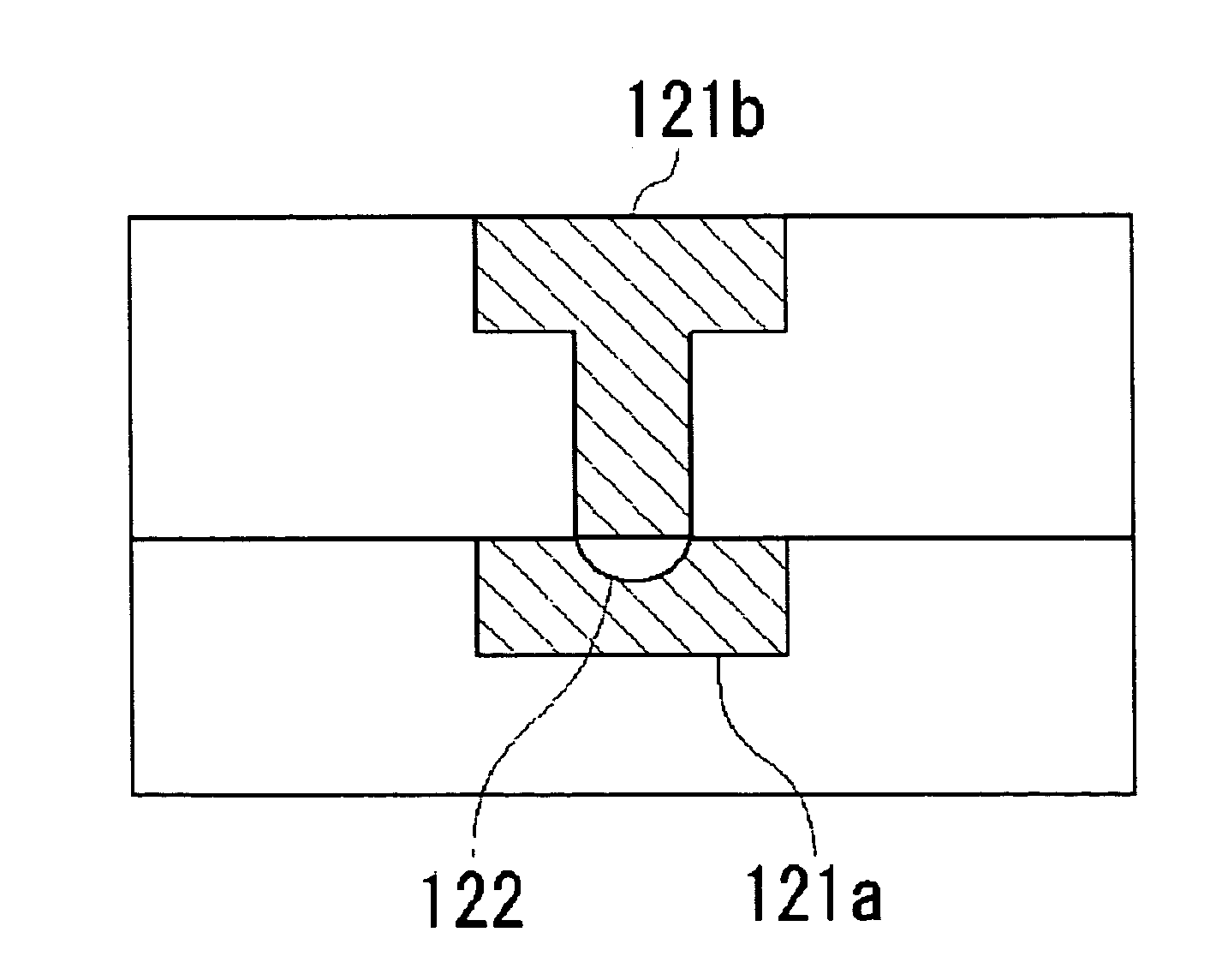
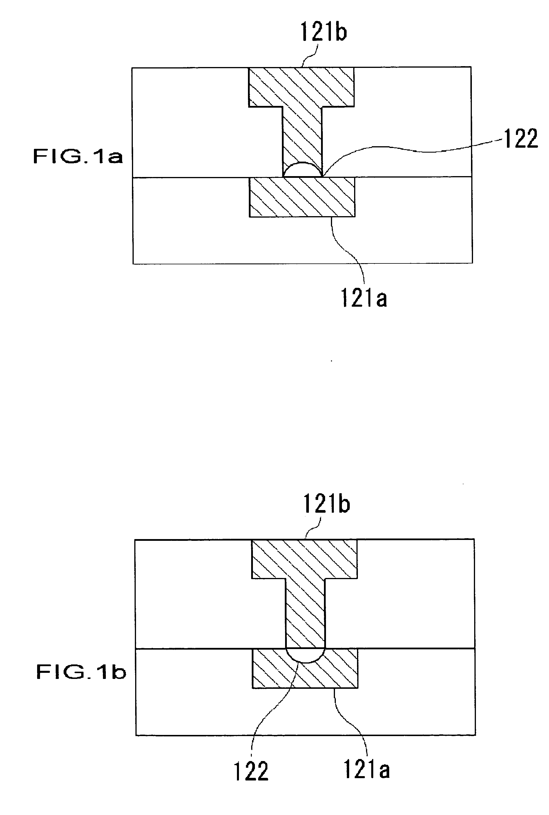
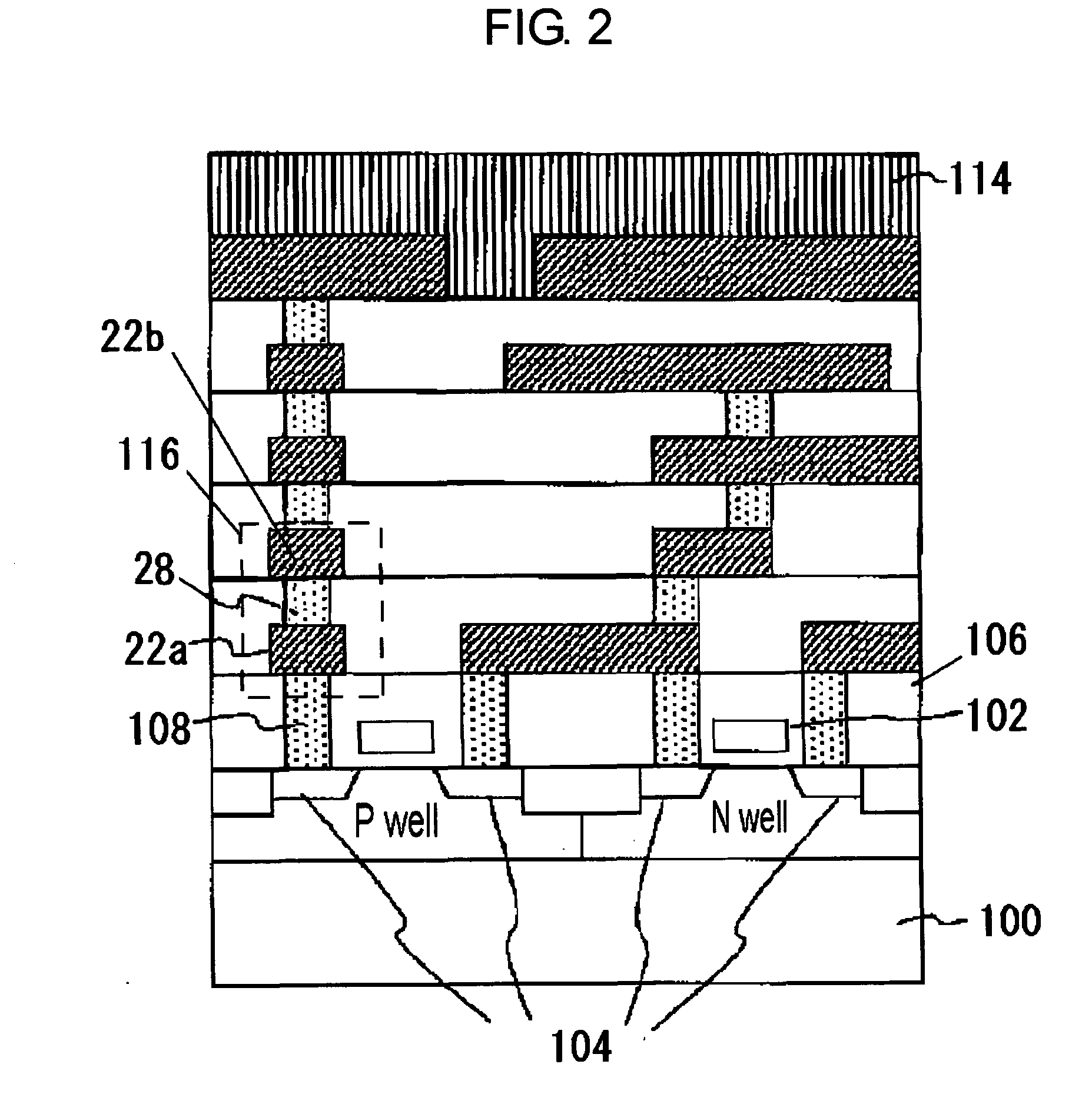
[0118] To start with, on the dielectric layer 106 formed on a silicon substrate (not shown), a first SiCN layer 12 (thickness approx. 70 nm) and a first HSQ layer 14a (thickness approx. 700 nm) are formed, on which a resist layer (not shown) patterned in a prescribed design is then provided, and progressive etching is performed on the first SiCN layer 12 and the first HSQ layer 14a to form an interconnect trench (FIG. 3a).

[0119] Then Ta and TaN are layered by sputtering and reactive sputtering to form a tantalum family barrier metal layer 24a (thickness of Ta approx. 20 nm, that of TaN approx. 10 nm) all over the substrate (FIG. 3b).

[0120] Following the above a seed copper-containing metal layer 60 (approx. 100 nm thick) is formed by sputtering over the tantalum family barri...

second embodiment

[0136] Second Embodiment

[0137] The second embodiment is different from the first embodiment in that a CVD copper layer 68 is formed by plasma CVD method instead of forming the seed copper-containing metal layer 60 and the plated copper layer 62, when forming the first copper-containing metal interconnect 22a, the connecting plug 28 and the second copper-containing metal interconnect 22b.

[0138] This embodiment shall be described referring to FIGS. 6 and 7. After forming the tantalum barrier metal layer 24a, the CVD copper layer 68 (thickness approx. 200 nm at a plain portion) is formed by plasma CVD method (FIG. 6a). At this stage, crystal orientation of the CVD copper layer 68 is (111). It is preferable to form the CVD copper layer 68 in such a thickness that does not completely fill the interconnect trench.

[0139] Then, copper oxide on a surface of the CVD copper layer 68 is sputtered and reduced by Ar / H.sub.2 plasma of a room temperature in a cleaning chamber. And then the substrat...

third embodiment

[0148] Third Embodiment

[0149] The third embodiment is different from the first embodiment in that the connecting plug 28 and the second copper-containing metal interconnect 22b by dual Damascene method. Referring to FIGS. 8 and 9, similar components to those in FIGS. 3 to 5 referred to in the first embodiment are given the identical numerals, and description thereof shall be omitted as the case may be.

[0150] The first copper-containing metal interconnect 22a can be formed in a similar manner to the preceding description of the first embodiment referring to FIG. 3, or to the following description on the second copper-containing metal interconnect 22b.

[0151] After forming the first copper-containing metal interconnect 22a (FIG. 8a), the second SiCN layer 16 and a silicon oxide layer 50 are deposited (FIG. 8b). Then progressive etching is performed on the silicon oxide layer 50 utilizing lithography method, to form a connecting hole 52 and an interconnect trench 52 for the connecting p...


PUM

PropertyMeasurementUnit
grain sizeaaaaaaaaaa
sizeaaaaaaaaaa
widthaaaaaaaaaa

Abstract

An interconnect trench is formed on a dielectric layer 12 and a first HSQ layer 14 formed on a semiconductor substrate, and a tantalum family barrier metal layer 24a is formed all over the substrate. Then a seed copper-containing metal layer 60 and a plated copper layer 62 are formed so as to fill a part of the interconnect trench. After that, a bias-sputtered copper-containing metal layer 64 is formed on the plated copper layer 62 so as to fill the remaining portion of the interconnect trench and then heat treatment is performed. As a result, a dissimilar metal contained in the bias-sputtered copper-containing metal layer 64 diffuses uniformly into the plated copper layer 62.

Description

[0001] This application is based on Japanese patent application NO.2002-198432, the content of which is incorporated hereinto by reference.[0002] 1. Field of the Invention[0003] The present invention relates to a semiconductor device and a manufacturing method thereof.[0004] 2. Description of the Related Art[0005] In accordance with the recent growing demand for a higher integration level of a semiconductor device, copper has come to be more extensively used as a material for an interconnect, a plug, a pad and so on. Copper has lower electrical resistance and better electromigration resistance than aluminum, which has been conventionally employed.[0006] However, along with a further progress in micronization of elements, electromigration (hereinafter referred to as "EM") has once again become a problem to be eliminated, even with a copper interconnect. A copper layer constituting a copper interconnect, generally formed by plating, consists of a number of combined copper grains of a ...

Claims


Application Information

Patent Timeline
Patent Type & Authority Applications(United States)
IPC IPC(8): H01L21/285H01L21/3205H01L21/288H01L21/60H01L21/768H01L23/52H01L23/532
CPCH01L21/2855H01L21/2885H01L2924/0002H01L2924/13091H01L2224/0401H01L21/76843H01L21/76858H01L21/76864H01L21/76873H01L21/76874H01L21/76877H01L21/76883H01L21/76886H01L23/53238H01L24/11H01L2224/05567H01L2224/13022H01L2224/13099H01L2924/01004H01L2924/01012H01L2924/01013H01L2924/01018H01L2924/01022H01L2924/01027H01L2924/01029H01L2924/0103H01L2924/01033H01L2924/0104H01L2924/01042H01L2924/01046H01L2924/01047H01L2924/01073H01L2924/01074H01L2924/01078H01L2924/01079H01L2924/01082H01L2924/01327H01L2924/04953H01L2924/19043H01L2924/3011H01L2924/01005H01L2924/01006H01L2924/01024H01L2924/01041H01L2924/014H01L2924/00H01L2224/05552H01L2224/05147H01L2224/05166H01L2224/05666H01L2224/05124H01L24/05H01L24/13H01L24/03H01L2924/00014H01L2924/013
Inventor KUNISHIMA, HIROYUKITAKEWAKI, TOSHIYUKI
Owner RENESAS ELECTRONICS CORP
Why Eureka
Try Eureka